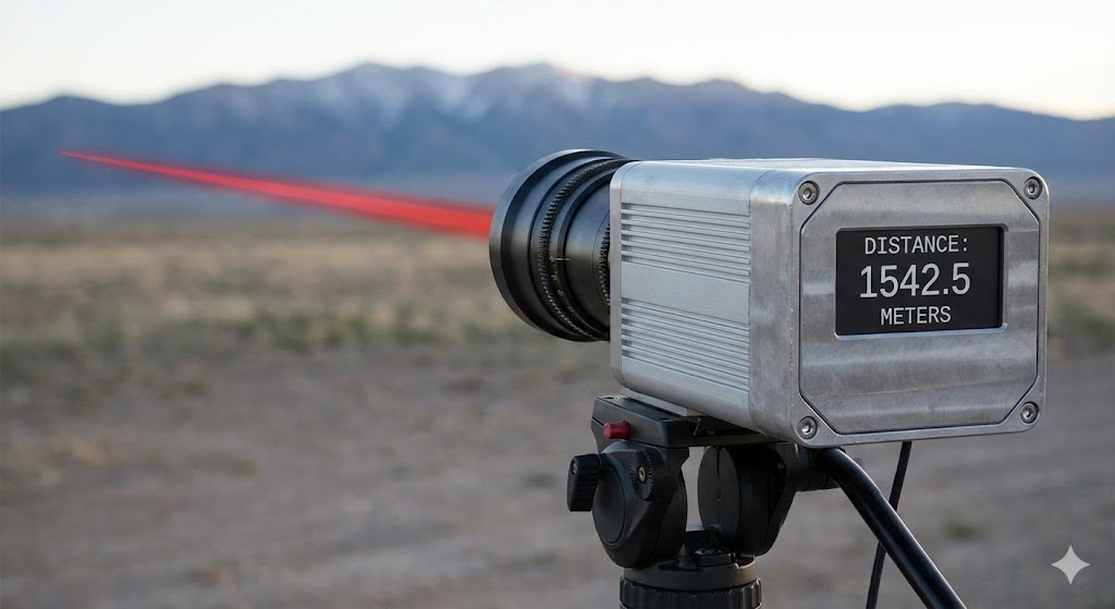
In the realm of modern electronics and imaging systems, the Complementary Metal-Oxide-Semiconductor (CMOS) sensor has become ubiquitous. From smartphone cameras to advanced machine vision systems in industrial automation, these sensors are the eyes of countless devices. However, a significant and often underappreciated vulnerability exists: their acute sensitivity to laser radiation. For electrical engineers and system designers, understanding this vulnerability is not merely academic; it is critical for ensuring reliability, safety, and longevity in applications ranging from consumer electronics to aerospace.
At its core, a CMOS image sensor is an integrated circuit containing an array of photodiodes (pixels). Each photodiode converts incoming photons into an electrical charge. This process relies on the photoelectric effect within a silicon substrate. The intricate structure includes microlenses, color filters, and, most importantly, sensitive semiconductor junctions. When exposed to normal light levels, this system functions predictably. However, a laser presents a fundamentally different threat profile due to its properties of coherence, monochromaticity, and high energy density.
The primary mechanism of damage is thermal. A focused laser beam delivers a high power density (watts per square centimeter) to a minuscule area on the sensor surface. Silicon, while a good semiconductor, has a finite absorption coefficient for specific laser wavelengths. The absorbed energy is converted into heat almost instantaneously. This localized heating can cause several catastrophic failures. At temperatures exceeding the silicon's melting point (approximately 1414°C), the photodiode structure itself can be physically destroyed, creating a dead pixel or cluster. Even below the melting point, thermal stress can induce delamination of micro-lenses or filters, and create lattice defects in the silicon crystal, leading to increased dark current and permanent "hot" pixels.
A second, more subtle mechanism is electro-optical overload or latch-up. The intense photon flux from a laser can generate a massive surge of photocurrent within the pixel's photodiode and the adjacent readout circuitry. This can overwhelm the designed charge-handling capacity (the full-well capacity), causing blooming (charge spilling into adjacent pixels) and complete saturation. In severe cases, this current surge can trigger a parasitic silicon-controlled rectifier (SCR) effect within the CMOS structure—a condition known as latch-up. This creates a low-impedance path between the power supply and ground, leading to excessive current flow, localized overheating, and potentially permanent damage to the transistor circuitry, even if the laser exposure is brief.
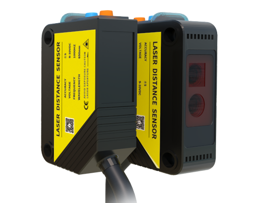
The risk profile varies significantly with laser parameters. Wavelength is paramount. Lasers in the visible and near-infrared spectrum (e.g., 532nm green, 650nm red, 808nm IR) are highly absorbed by silicon and are particularly dangerous. Pulse duration is equally critical. A high-energy, short-pulse laser (nanosecond or picosecond pulses) can cause dielectric breakdown through avalanche ionization before significant heat diffusion occurs, ablating material. Continuous-wave (CW) lasers cause predominantly thermal damage. Furthermore, the sensor's operational state matters; a sensor actively reading out data during exposure is often more susceptible to latch-up events.
For engineers designing systems that may encounter laser hazards—such as LiDAR systems, laser rangefinders, surgical equipment, or even devices in public spaces—mitigation strategies are essential. Optical filtering is the first line of defense. Installing band-pass or notch filters that block specific laser wavelengths while passing the desired imaging spectrum can dramatically reduce incident energy. However, filters have limitations in blocking very high-power or broad-wavelength threats. Physical barriers and apertures can be used to limit the field of view and reduce the chance of direct beam entry.
At the circuit design level, incorporating robust protection diodes and designing for higher latch-up immunity in the CMOS fabrication process are crucial. Implementing software-based safeguards, such as real-time pixel anomaly detection that can identify and correct for suddenly saturated or dead pixels, can help maintain system functionality after a non-catastrophic event. For critical applications, system-level redundancy, using multiple sensors with physical separation, may be necessary.
In conclusion, the vulnerability of CMOS sensors to laser damage is a well-defined phenomenon rooted in the physics of semiconductors and optical energy interaction. It is not a design flaw but an inherent characteristic of the technology. For the practicing electrical engineer, dismissing this vulnerability can lead to field failures with serious consequences. A proactive approach, combining an understanding of the failure mechanisms with a layered defense strategy encompassing optical, electronic, and software solutions, is imperative. As laser technology becomes more pervasive, designing CMOS-based systems with laser robustness in mind will transition from a niche consideration to a standard engineering practice, ensuring that these essential "eyes" of technology can see clearly and reliably, even in potentially hostile optical environments.