In the rapidly evolving landscape of electrical engineering and industrial automation, laser CMOS sensors have emerged as a cornerstone technology for precision measurement, object detection, and quality control. These sophisticated devices integrate the coherent, monochromatic light of a laser source with the high-speed, low-power imaging capabilities of a Complementary Metal-Oxide-Semiconductor (CMOS) sensor. The fundamental principle hinges on the precise interaction between emitted laser light and a target object, with the CMOS array capturing the resultant optical information for digital processing.
The operational cycle begins with the laser diode, which emits a focused beam of light, typically in the visible red or infrared spectrum. This laser light is characterized by its low divergence, high intensity, and specific wavelength, making it ideal for creating a sharp, defined point or line profile on a target surface. When this structured light pattern strikes an object, several optical phenomena occur: reflection, scattering, and potentially diffraction. The key measured parameters are often the position, intensity, or phase shift of the reflected light.
The heart of the system is the CMOS image sensor. Unlike its CCD (Charge-Coupled Device) predecessor, a CMOS sensor is an active pixel sensor where each photosite contains its own amplifier and analog-to-digital conversion circuitry. This architecture allows for faster readout speeds, lower power consumption, and greater integration flexibility. The sensor's pixel array is precisely aligned to capture the laser's projection. In a basic triangulation-based distance sensor, for example, the laser dot's position on the CMOS array shifts linearly as the target object's distance changes. A closer object causes the reflected dot to shift its position on the sensor plane in one direction, while a farther object causes a shift in the opposite direction. The onboard processor, often a dedicated microcontroller or FPGA, calculates this displacement in real-time using calibrated algorithms to determine exact distance with micron-level resolution.

More advanced configurations utilize laser line projection for 3D profiling. Here, a laser line generator projects a thin plane of light onto an object. The CMOS camera, positioned at a known angle, captures the contour of this line as it deforms over the object's surface. By analyzing the distortion of this line across thousands of points simultaneously, the sensor can construct a detailed height map or 3D point cloud. This principle is fundamental in applications like surface inspection, robotic bin picking, and volume measurement.
The integration of the laser and CMOS components demands meticulous optical design. Lenses are used to collimate the laser beam and to focus the reflected light onto the sensor array. Optical filters are critical, especially in industrial environments; a narrow bandpass filter tuned to the laser's wavelength is placed in front of the CMOS sensor. This filter dramatically attenuates ambient light (e.g., factory lighting, sunlight), allowing only the laser's specific frequency to pass through. This significantly enhances the signal-to-noise ratio, enabling reliable operation in challenging lighting conditions.
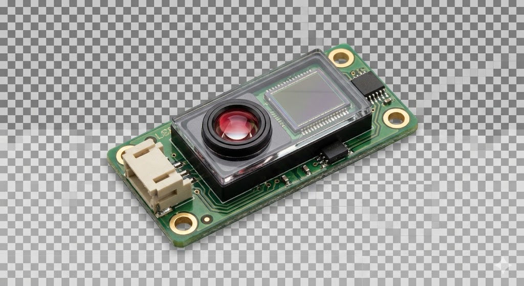
Signal processing is the final, crucial layer. The raw analog signal from each CMOS pixel is converted to a digital value. Sophisticated firmware then executes algorithms for tasks like peak detection (finding the brightest point of the laser dot), sub-pixel interpolation for enhanced accuracy, and noise reduction. For complex measurements like width or presence detection, the system evaluates the intensity profile across a row of pixels, setting thresholds to determine edges or object boundaries.
The advantages of laser CMOS sensors are manifold. They offer non-contact measurement, eliminating mechanical wear and allowing inspection of delicate materials. Their high speed and accuracy are unparalleled for dynamic processes. The CMOS technology itself enables compact, cost-effective, and robust designs suitable for harsh industrial environments. From monitoring the thickness of rolled steel in a mill and guiding autonomous mobile robots on a factory floor to ensuring the precise assembly of microelectronics, these sensors are indispensable.
Future trends point toward further miniaturization, the use of novel laser wavelengths like VCSELs (Vertical-Cavity Surface-Emitting Lasers), and deeper integration of artificial intelligence directly at the sensor level for adaptive, smart sensing. Understanding the core principles of laser emission, structured light interaction, and CMOS-based photoelectric conversion is essential for any engineer designing the next generation of automated, intelligent systems. The synergy of these technologies continues to push the boundaries of what is measurable and controllable in the physical world.