Laser sensors represent a critical technology across numerous industries, from automotive and aerospace to consumer electronics and industrial automation. Their ability to provide precise, non-contact measurement and detection makes them indispensable. The manufacturing of these sophisticated devices is a multi-stage, highly controlled process that ensures reliability, accuracy, and performance. This article details the standard manufacturing process flow for a typical laser sensor, outlining each critical step from initial design to final testing and packaging.
The journey begins with the Design and Prototyping Phase. Engineers develop detailed schematics and specifications based on the sensor's intended application—whether for distance measurement, object detection, or profile scanning. This phase involves extensive computer-aided design (CAD) and simulation to model the sensor's optical path, electronic circuitry, and mechanical housing. Key components like the laser diode (often a VCSEL or edge-emitting laser), photodetector (such as a PIN photodiode or CMOS array), and focusing lenses are selected. A functional prototype is then built and rigorously tested to validate the design against performance criteria. Any issues with signal-to-noise ratio, range, or environmental stability are addressed through iterative design refinements.
Following design validation, the process moves to Component Sourcing and Inspection. High-purity materials and precision components are procured from qualified suppliers. The laser diode, the heart of the sensor, is sourced for specific wavelength (commonly 650nm, 850nm, or 905nm) and output power. Optical elements like lenses and filters are inspected for surface quality and precise focal lengths. Electronic components, including the driver IC for the laser and the amplifier for the detector, are acquired. Incoming materials undergo a stringent quality inspection, using tools like optical microscopes and electrical testers, to ensure they meet the exact tolerances required for high-performance sensor assembly.
The core of the manufacturing flow is the Assembly and Integration Stage, which is typically performed in a cleanroom environment to prevent particulate contamination. This stage is often subdivided into sub-module assembly:

1. Optical Sub-Assembly: The laser diode is precisely aligned and mounted onto a submount or heatsink. Collimating or focusing lenses are then aligned in the optical path to shape the laser beam. This alignment, often done with active feedback using a power meter or position sensor, is crucial for beam quality and must be permanently fixed using laser welding or UV-curing epoxy.
2. Detector Sub-Assembly: The photodetector is similarly mounted and aligned, often with its own set of lenses or filters to optimize light reception and reject ambient noise.
3. PCB Assembly: The printed circuit board (PCB), which hosts the laser driver, signal processing circuitry, microcontroller, and communication interfaces, is populated using Surface Mount Technology (SMT). Automated pick-and-place machines and reflow ovens ensure consistent and reliable soldering of miniature components.
4. Final Integration: The optical sub-assembly, detector sub-assembly, and populated PCB are integrated into a single mechanical housing. This housing provides structural integrity, protects the delicate internals, and may include features for heat dissipation. Precise mechanical fixtures are used to ensure the final alignment between the emitted laser beam and the receiver's field of view. The unit is then sealed, often with gaskets or epoxy, to achieve the desired Ingress Protection (IP) rating for dust and water resistance.
Once assembled, the sensor enters the Calibration and Testing Phase, arguably the most critical for ensuring performance. Each unit undergoes a battery of automated tests:
* Functional Testing: The sensor is powered on, and basic operations are verified.
* Optical Power and Safety Check: Laser output power is measured to ensure it is within specified and eye-safe limits (complying with standards like IEC 60825-1).
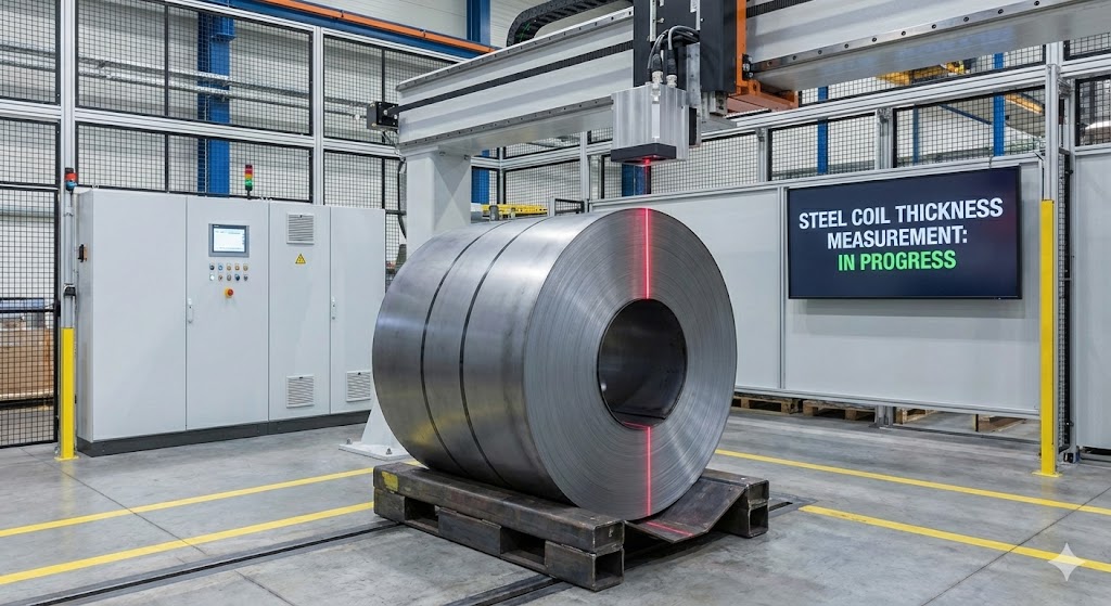
* Metrological Calibration: The sensor is tested against known reference distances or targets. Correction factors and calibration coefficients are calculated and programmed into the sensor's non-volatile memory. This step compensates for minor component variances and ensures measurement accuracy across the entire operating range.
* Environmental Stress Screening: A sample from each production batch may be subjected to temperature cycling, humidity tests, and vibration tests to validate robustness and long-term reliability.
The final step is Finalization and Packaging. Sensors that pass all tests are labeled with serial numbers for traceability. They are then carefully packaged in anti-static materials to prevent damage during shipping. The packaging often includes necessary accessories like mounting brackets, cables, and user documentation. The entire batch is documented, and a certificate of conformity may be issued before the products are shipped to distributors or end customers.
In conclusion, the manufacturing of laser sensors is a complex symphony of optical engineering, precision mechanics, and electronics assembly. Each step in the process flow, from meticulous design to rigorous final testing, is essential to produce a device that delivers consistent, accurate, and reliable performance in the field. This controlled, multi-stage approach is what allows laser sensor technology to be deployed confidently in mission-critical applications worldwide.