Introduction to Photoelectric Sensor Architecture
Photoelectric sensors are essential components in industrial automation, used for detecting objects, distances, or positions without physical contact. A typical photoelectric sensor’s block diagram reveals its core functional modules: emitter, receiver, signal processing unit, output driver, and power supply. This article provides an in-depth look at each block in a photoelectric sensor block diagram, tailored for electrical engineers who design or troubleshoot these systems.
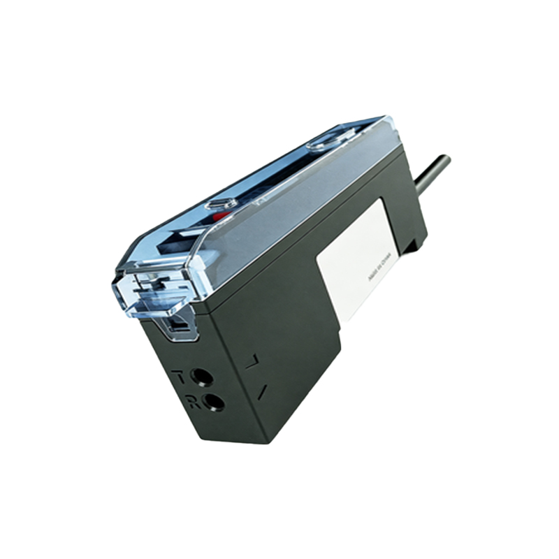
Emitter Block: Light Source and Modulation
The emitter block generates the light beam, usually from an LED (infrared, red, or laser). In a block diagram, this includes a driver circuit that modulates the light at a specific frequency (e.g., 1-10 kHz) to reject ambient light noise. The emitter may integrate a lens to collimate or focus the beam. Engineers must consider factors like wavelength (for material penetration) and modulation depth to ensure reliable detection in dusty or humid environments.
Receiver Block: Photodetector and Preamplifier
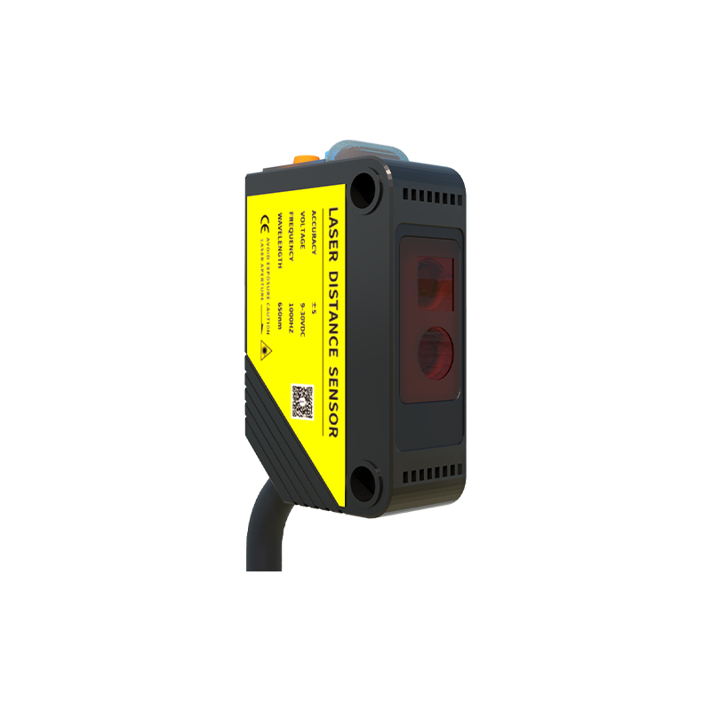
The receiver block comprises a photodiode or phototransistor that converts incoming light into a current signal. This is followed by a preamplifier (transimpedance amplifier) that converts the small current into a voltage. The block diagram often shows a bandpass filter tuned to the emitter’s modulation frequency, which suppresses interference from sunlight or artificial lighting. Key design parameters include responsivity (A/W), dark current, and signal-to-noise ratio (SNR).
Signal Processing Block: Demodulation and Threshold Comparison
After preamplification, the signal enters the processing block. Here, a demodulator extracts the modulated component from the received light. A comparator then compares the demodulated signal against a preset threshold voltage, which determines the sensing distance and hysteresis. Some advanced sensors include an analog-to-digital converter (ADC) for digital processing, enabling adaptive thresholding or background suppression. The block diagram may show a microcontroller (MCU) for configuration.
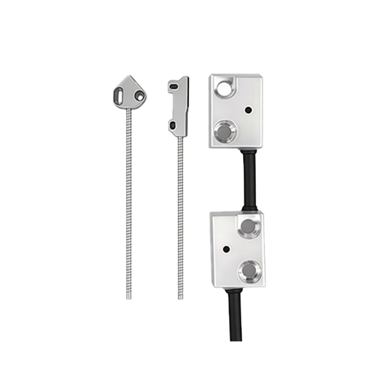
Output Driver Block: Switching and Output Types
The output driver block interfaces with the control system. Common outputs are NPN/PNP transistor switches, relay contacts, or push-pull outputs. In the block diagram, this stage includes a transistor driver, short-circuit protection, and an output indicator LED. Engineers must match the output type to the PLC input module (sink/source logic) and consider load current ratings (typically 100-200 mA). A status LED is often integrated for visual feedback.
Power Supply Block: Regulation and Noise Filtering
The power supply block converts the input voltage (e.g., 10-30 VDC) into regulated voltages for internal circuits. This includes a voltage regulator (linear or switching) and decoupling capacitors to filter high-frequency noise. In industrial environments, transient protection (e.g., TVS diodes) and reverse polarity protection are critical. The block diagram should show separate supply rails for analog and digital sections to minimize crosstalk.
Integration and Practical Considerations
When designing or analyzing a photoelectric sensor block diagram, engineers should test key points: emitter current (to verify light output), receiver preamplifier output (for signal amplitude), and comparator threshold voltage. Environmental factors like temperature drift and vibration also affect performance. Advanced sensors may include self-diagnostics and IO-Link communication, which add a digital interface block to the diagram. Understanding these blocks enables efficient troubleshooting and customization for specific applications such as conveyor systems, packaging, or safety light curtains.