Introduction to Photoelectric Sensors and Photosensitive Film
Photoelectric sensors are essential components in industrial automation, detecting objects or changes in light intensity. The core of these sensors lies in the photosensitive film, a thin layer that converts light energy into electrical signals. This article delves into the principle diagram of the photosensitive film, explaining its operational mechanics in a professional electrical engineering context.
Basic Structure of the Photosensitive Film
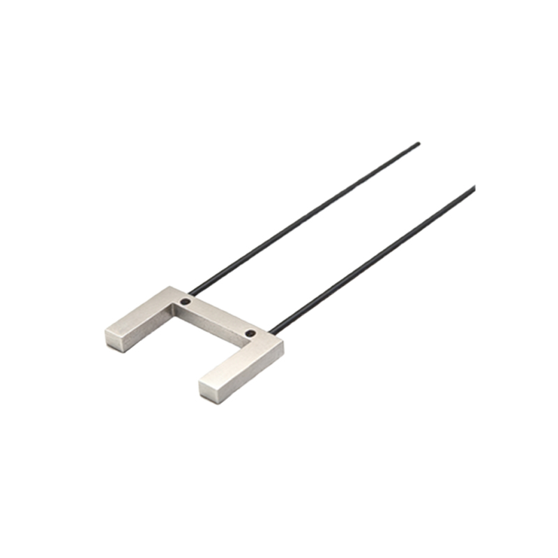
The photosensitive film typically consists of a semiconducting material, such as cadmium sulfide (CdS) or amorphous silicon, deposited on a substrate. The diagram shows the film sandwiched between two conductive electrodes: a transparent top electrode (e.g., indium tin oxide) and a bottom metal electrode. When light strikes the film, photons with sufficient energy excite electrons from the valence band to the conduction band, creating electron-hole pairs.
Working Principle in the Diagram
The principle diagram illustrates the photoconductive effect. In the absence of light, the film exhibits high resistance due to the lack of free charge carriers. Upon illumination, the generated electron-hole pairs increase conductivity. The circuit includes a biasing voltage applied across the electrodes. As light intensity rises, the current flowing through the film increases proportionally, which is measured as a voltage drop across a load resistor. The diagram typically includes a schematic of a photoconductive cell with labeled components: light source, photosensitive film, power supply, and output signal.
Key Electrical Characteristics
The diagram also highlights parameters like responsivity (A/W), response time, and spectral sensitivity. Responsivity defines the electrical output per unit of incident light power. For industrial applications, the film must have fast response times to detect rapid movements. The graph on the diagram shows the spectral response curve, peaking at specific wavelengths (e.g., 550 nm for visible light sensors). Engineers use this to match the sensor to the light source.
Circuit Integration and Output Signal Processing
In the principle diagram, the photosensitive film is part of a comparator circuit or an amplifier stage. The output from the film is fed into a Schmitt trigger to eliminate noise and produce a clean digital signal. Alternatively, for analog applications, a transimpedance amplifier converts the photocurrent into a voltage. The diagram includes a transistor or op-amp configuration, with feedback components to stabilize gain and frequency response.
Practical Considerations for Industrial Use
The diagram must account for environmental factors like temperature drift and ambient light interference. A common design includes a shielding layer to block unwanted wavelengths. For high-precision tasks, the film is often encapsulated in a hermetic package. Engineers also consider the fatigue effect, where prolonged exposure to high light levels degrades the film's sensitivity. The principle diagram typically adds a reference photodiode for calibration.
Conclusion and Application Example
Understanding the principle diagram is crucial for troubleshooting and optimizing photoelectric sensors. For instance, in a conveyor belt system, the photosensitive film detects package presence. The diagram helps adjust the threshold voltage to avoid false triggers. By studying the film's electrical response, engineers can improve sensor reliability in dusty or humid environments.