Perovskite-based photoelectric sensors have emerged as a transformative technology in the electrical engineering sector, offering superior sensitivity and cost-effectiveness compared to traditional silicon-based sensors. These sensors utilize perovskite materials—a class of compounds with a distinctive crystal structure—to convert light into electrical signals with high efficiency. Their unique optoelectronic properties, including tunable bandgaps and high absorption coefficients, make them ideal for industrial automation, environmental monitoring, and precision measurement systems.
Key Performance Metrics and Material Advantages
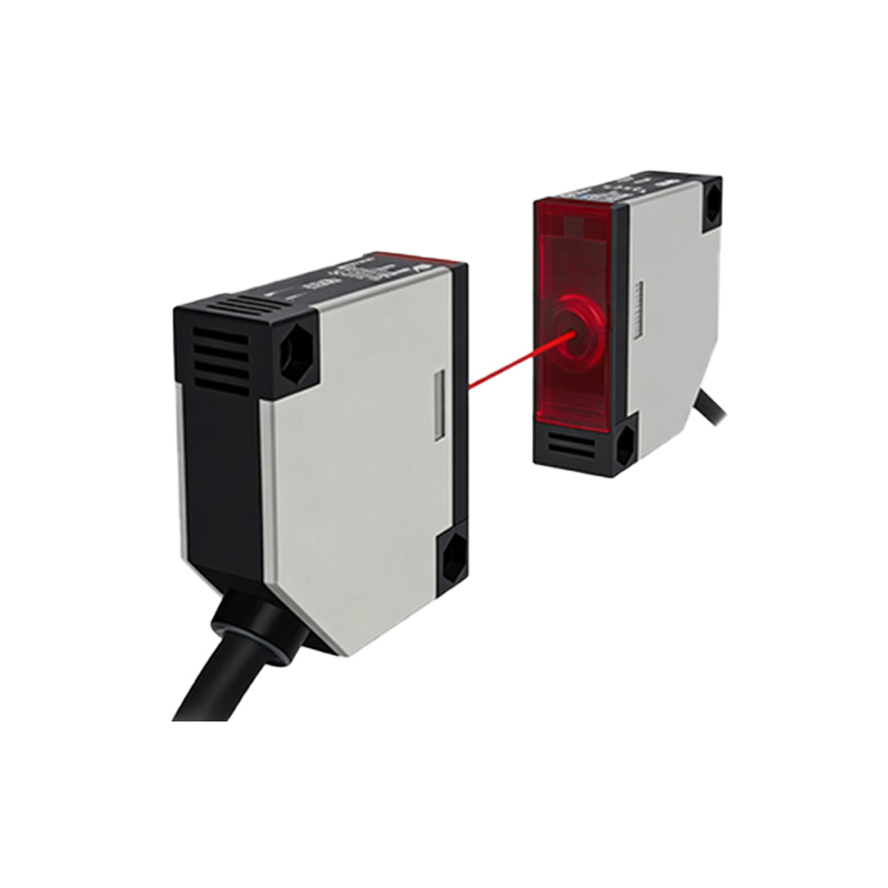
The performance of perovskite photoelectric sensors is defined by several critical metrics: responsivity, detectivity, response time, and stability. Recent engineering advancements have achieved responsivity values exceeding 10 A/W under low-light conditions, significantly outperforming organic photodetectors. The material's defect tolerance and solution-processability allow for scalable manufacturing on flexible substrates, enabling integration into curved or compact industrial equipment. Additionally, the bandgap tunability from 1.2 eV to 2.3 eV facilitates custom spectral responses for applications like infrared thermography or ultraviolet dosimetry.
Engineering Challenges and Reliability Solutions
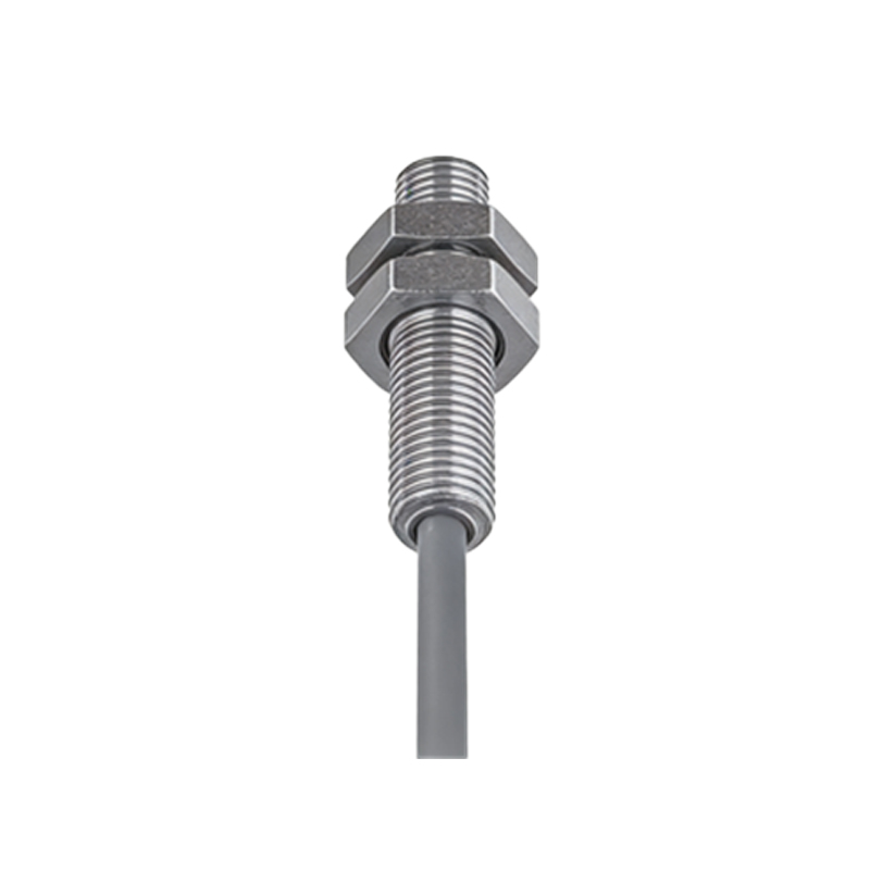
Despite their promise, perovskite sensors face hurdles in long-term operational stability, particularly under high humidity or temperature fluctuations common in industrial environments. Current research focuses on encapsulation techniques using barrier layers such as atomic-layer-deposited aluminum oxide to mitigate degradation. Furthermore, lead-free alternatives like tin-based perovskites are being developed to comply with RoHS directives while maintaining competitive performance. Engineers are also optimizing interface engineering to reduce dark current noise, achieving noise-equivalent power values below 10^-12 W/Hz^0.5.
Integration with Industrial IoT Systems
Perovskite photoelectric sensors are now being integrated into Industrial Internet of Things (IIoT) frameworks. Their low power consumption (operating at<1 µW) and fast response times (sub-millisecond) make them suitable for real-time data acquisition in smart factories. For example, in automated optical inspection systems, these sensors detect minute defects in semiconductor wafers with over 95% accuracy. Their compatibility with wireless communication protocols like LoRaWAN enables remote monitoring of light-based parameters in hazardous environments.
Future Outlook and Research Directions
The next decade will see perovskite sensors pushing boundaries in spectral imaging and multi-modal detection. Emerging morphologies include 2D perovskite heterostructures for enhanced charge carrier mobility and quantum dot composites for near-infrared sensitivity. Industry collaborations aim to standardize reliability testing protocols, while machine learning algorithms are being employed to compensate for sensor drift. As production yields improve, the cost per unit is projected to drop below $0.50, democratizing access to high-performance sensing across the electrical industry.