Introduction to Photosensitive Film in Photoelectric Sensors
The photosensitive film, also known as the photoelectric layer or photodetector coating, is a critical component in photoelectric sensors. It is a thin semiconductor material that converts light energy into an electrical signal. This film is typically deposited on a substrate within the sensor's receiver, such as a phototransistor or photodiode. Its primary function is to detect changes in light intensity, wavelength, or presence, enabling the sensor to perform tasks like object detection, counting, or positioning in industrial automation systems. As an electrical engineer, understanding its material composition, operational principles, and failure modes is essential for designing reliable sensing circuits.
Material Composition and Fabrication
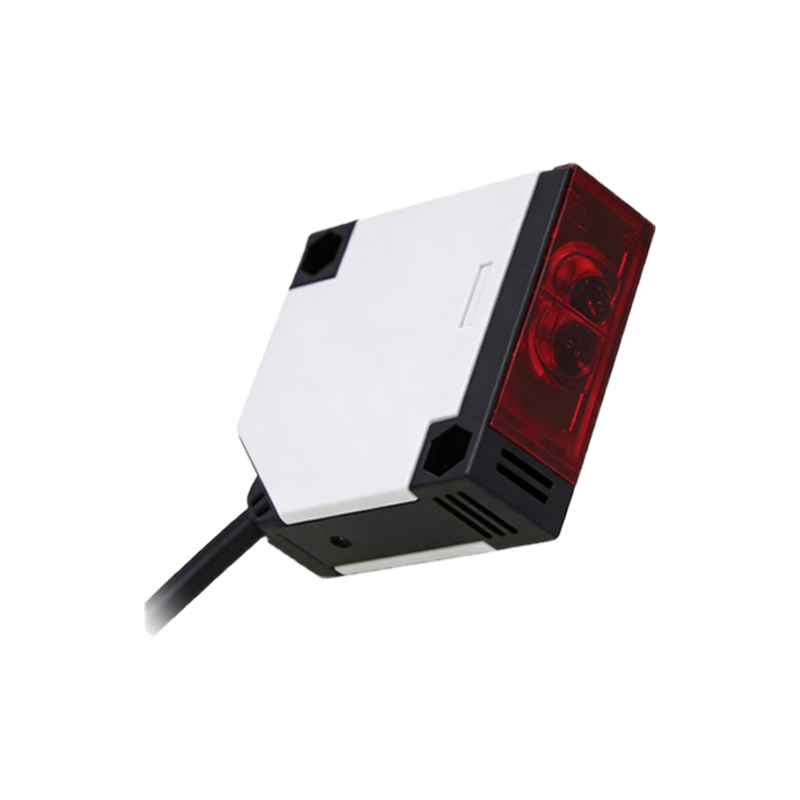
Photosensitive films are often made from semiconductor materials like silicon (Si), gallium arsenide (GaAs), or indium gallium arsenide (InGaAs). Silicon-based films are common for visible and near-infrared light, while compound semiconductors like InGaAs are used for longer wavelengths. The film is fabricated using deposition techniques such as chemical vapor deposition (CVD) or sputtering, resulting in a layer thickness ranging from a few micrometers to tens of micrometers. The film's surface may be textured or coated with anti-reflective layers to enhance quantum efficiency. For high-speed applications, materials like amorphous silicon or organic photoconductors are selected for their fast response times.
Operational Principle: From Photons to Electrons
When photons strike the photosensitive film, they excite electrons from the valence band to the conduction band, generating electron-hole pairs. This phenomenon, known as the photoelectric effect, creates a photocurrent proportional to the incident light intensity. The film's internal electric field, often aided by a reverse bias voltage, separates these carriers, producing a measurable current or voltage change. The sensor's output signal is then processed by a comparator or amplifier circuit. Key parameters include responsivity (A/W), dark current (leakage current in absence of light), and response time (typically nanoseconds to microseconds). Engineers must consider these factors when matching the sensor to specific light sources, such as LEDs or laser diodes.
Performance Factors and Environmental Considerations
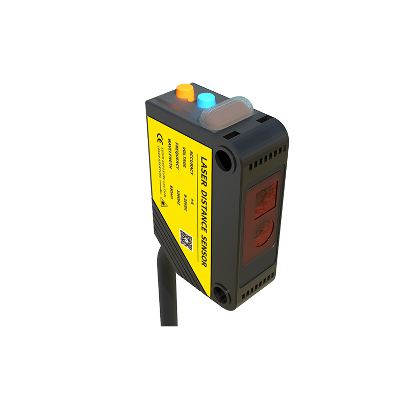
The performance of the photosensitive film is influenced by temperature, humidity, and contamination. High temperatures can increase dark current, reducing signal-to-noise ratio. Humidity may cause oxidation or delamination of the film, especially in unsealed sensors. Dust or oil on the film surface attenuates light and degrades sensitivity. To mitigate these issues, sensors often include protective windows, hermetic sealing, or temperature compensation circuits. For harsh industrial environments, films with passivation layers or rugged materials like silicon carbide (SiC) are preferred. Engineers should also account for aging effects, as repeated light exposure can degrade film efficiency over time.
Common Failure Modes and Troubleshooting
Typical failure modes include photodegradation, where the film's quantum efficiency decreases due to prolonged UV exposure; thermal damage from excessive heat; and electrical breakdown from overvoltage. Contamination or physical scratches can cause uneven sensitivity, leading to false triggers. To diagnose issues, measure the sensor's dark current and responsivity under controlled light conditions. For instance, if the output current is lower than expected at a fixed light intensity, the film may be degraded. Replacing the sensor or cleaning the optical path can restore performance. In design, adding optical filters or limiting the light source intensity can extend film life.
Advanced Applications and Future Trends
Beyond basic industrial sensors, photosensitive films are crucial in LiDAR, fiber optic communications, and biomedical imaging. Emerging trends include the use of perovskite materials for higher sensitivity and flexibility, as well as nanostructured films for enhanced light trapping. For high-speed automation, avalanche photodiode (APD) structures with specialized films offer single-photon detection. Engineers should stay updated on material innovations, such as 2D materials like graphene, which promise ultra-wideband response. When selecting a sensor, evaluate the film's spectral range, stability, and cost to optimize the system's overall performance.