Introduction to Mobile Photoelectric Sensor Lenses
Photoelectric sensors in mobile devices rely on precision lens optics to detect ambient light, proximity, and color. The lens is a critical component that focuses or diffuses light onto the sensor’s photodiode array, directly impacting signal accuracy and device performance. In modern smartphones, these lenses must balance miniaturization with high optical efficiency, often using advanced materials like polycarbonate or glass composites to withstand thermal and mechanical stress.
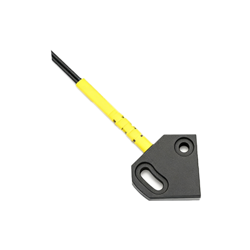
Key Design Parameters for Optical Performance
Lens design for mobile photoelectric sensors involves several key parameters: focal length, aperture size, and anti-reflective coatings. A shorter focal length enables compact modules, but requires aspherical lens shapes to reduce spherical aberration. Anti-reflective coatings, typically magnesium fluoride or multi-layer dielectric stacks, minimize light loss at the lens’s surface, improving sensitivity by up to 15%. Engineers must also account for the sensor’s spectral response, optimizing lens transmittance in the 400-700 nm visible range and near-infrared band for proximity sensing.
Material Selection and Manufacturing Challenges
High-index plastics, such as cyclic olefin copolymer (COC), are preferred for their low birefringence and high transmission. However, these materials are prone to scratch damage, necessitating hard-coat layers. Injection molding is the standard manufacturing process, achieving tolerances of ±0.005 mm. For high-volume production, multi-cavity molds reduce cycle time but require precise temperature control to prevent warping. Recent advances in 3D-additive manufacturing allow prototyping of custom lens arrays for flexible sensor configurations, though mass adoption remains limited due to surface roughness issues.
Emerging Trends: Miniaturization and Multi-Sensor Fusion
The demand for bezel-less displays drives lens diameters below 2 mm, challenging traditional fabrication methods. Wafer-level optics (WLO) enable batch production of micro-lens arrays directly on silicon substrates, aligning with CMOS sensor packaging. Additionally, multi-sensor fusion in devices like LiDAR scanners uses diffractive optical elements (DOEs) to split a single beam into multiple channels. These lenses must maintain low cross-talk below -30 dB to ensure accurate depth mapping. Thermal stability is another frontier—new glass-filled polymers expand by less than 10 ppm/°C, preventing focal shifts in extreme temperatures.
Performance Verification and Testing Protocols
Quality assurance includes modulation transfer function (MTF) testing at 50% contrast to evaluate resolution. For mobile lenses, MTF values above 0.6 at 20 lp/mm are typical. Transmission efficiency is measured using an integrating sphere with a calibrated photodiode. Industry standards, such as IEC 61290-6, dictate environmental stress tests including thermal cycling (-40°C to +85°C) and humidity exposure (95% RH). Automated visual inspection systems using machine learning identify defects like bubbles or scratches, achieving a false rejection rate lower than 0.1%.