1. Introduction to Photoelectric Sensors in Printers
Photoelectric sensors are critical components in modern printers, enabling precise detection of paper position, toner levels, and mechanical alignment. From an electrical engineering standpoint, these sensors convert light signals into electrical signals, which are then processed by the printer’s control system. Understanding the structure diagram of such sensors is essential for troubleshooting, design, and optimization. This article provides a detailed breakdown of the typical photoelectric sensor architecture used in laser and inkjet printers, focusing on the key elements: emitter, receiver, optical path, and signal conditioning circuits.
2. Core Components: Emitter and Receiver
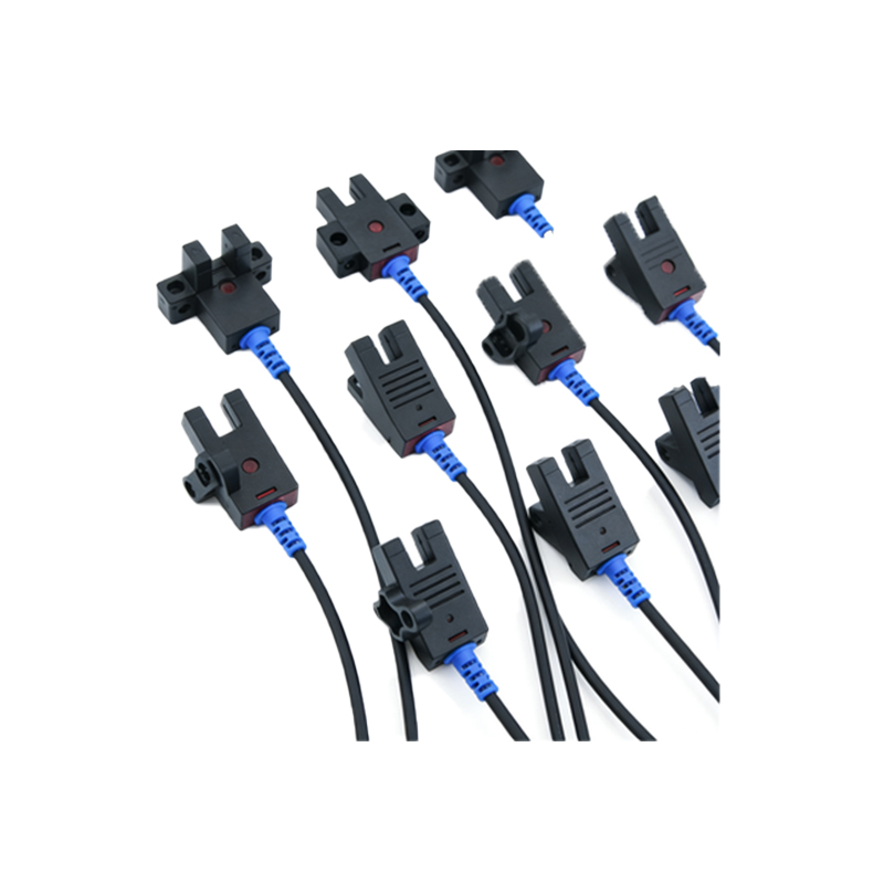
The sensor structure diagram typically features an infrared (IR) LED as the emitter and a phototransistor or photodiode as the receiver. The emitter generates a modulated light beam, often pulsed to reduce interference from ambient light. The receiver detects the reflected or transmitted light, depending on the sensor type (reflective or transmissive). In the diagram, these components are connected to a voltage source (Vcc) and a ground (GND), with the receiver’s output feeding into a comparator for signal processing. The emitter’s current is usually limited by a series resistor, values calculated based on LED specifications and desired intensity.
3. Optical Path and Mechanical Integration
The structure diagram includes an optical path that may involve lenses, apertures, or fiber optics to direct the light beam. In a printer, the sensor is often mounted near the paper path or toner cartridge. For example, a transmissive sensor uses a U-shaped slot where the paper interrupts the light beam between emitter and receiver, triggering a change in output voltage. The diagram shows the alignment of these optical elements, with critical distances marked (e.g., gap width of 2-5 mm). Engineers must consider contamination from toner dust or paper debris, which can degrade performance; thus, the design often includes a protective window or self-cleaning mechanism.
4. Signal Conditioning and Output Interface
Post-detection, the raw signal from the receiver is weak and noisy. The structure diagram illustrates a signal conditioning stage, typically a transimpedance amplifier (TIA) followed by a comparator with hysteresis. The TIA converts the photocurrent into a voltage, while the comparator produces a clean digital output (HIGH or LOW) corresponding to the presence or absence of the light beam. A reference voltage divider (using resistors R1 and R2) sets the threshold. In the diagram, the output pin (OUT) connects to the printer’s microcontroller via a pull-up resistor, ensuring compatibility with logic levels. Engineers often add a capacitor for filtering, with values ranging from 0.1 µF to 1 µF.
5. Common Failure Modes and Design Considerations
From an electrical engineering perspective, the structure diagram helps identify failure points: LED degradation (reduced light output), receiver saturation (due to excessive ambient light), or component drift (resistor tolerance). The diagram should include thermal management notes, as LED efficiency drops with temperature. For reliable operation, engineers specify components with wide operating voltage ranges (e.g., 3.3V to 5V) and low dark current. The physical layout in the diagram must avoid crosstalk between emitter and receiver, often achieved by a light-shielding barrier. Additionally, ESD protection diodes are recommended on the output line to prevent damage from static discharge during printer maintenance.
6. Practical Application: Interpreting the Diagram for Troubleshooting
When a printer exhibits paper jams or detection errors, the structure diagram serves as a roadmap. Engineers measure voltage at the receiver’s collector with a multimeter; a low voltage (e.g., 0.2V) when the beam is blocked indicates normal operation. If the output remains constant regardless of paper presence, the LED may be faulty, or the optical path is obstructed. The diagram helps trace the signal flow from emitter driver to comparator output. Using an oscilloscope at the test points marked in the diagram (TP1: emitter drive, TP2: receiver output) allows for dynamic analysis of pulse modulation. This systematic approach reduces repair time and improves printer reliability.