Introduction to Photoelectric Sensor SMD Technology
Photoelectric sensors are crucial components in modern automation systems, enabling precise detection of objects, distances, and color variations without physical contact. Surface-mount device (SMD) packaging has revolutionized the integration of these sensors into compact circuit boards, offering enhanced reliability and reduced footprint. In industrial environments, proper placement of photoelectric sensor SMD components is vital for maximizing performance, minimizing signal interference, and ensuring long-term durability. This article provides engineering insights into key considerations for SMD photoelectric sensor placement, covering layout, thermal management, and optical alignment.
Key Factors in SMD Placement for Optical Performance
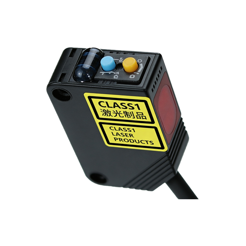
The optical performance of photoelectric sensors heavily depends on the alignment and positioning of the SMD package. Engineers must ensure that the light-emitting and receiving elements are unobstructed by adjacent components, such as capacitors or resistors, which could cast shadows or scatter light. A clear line-of-sight path from the sensor to the target is essential. Additionally, the placement should account for ambient light interference—avoiding positioning near bright LEDs or reflective surfaces that could trigger false readings. Using a 3D layout simulation tool during the PCB design phase can identify potential optical obstructions before manufacturing.
Thermal Management Considerations for Sensor Reliability
Photoelectric sensors generate heat during operation, and improper heat dissipation can degrade sensitivity or cause premature failure. When placing SMD photoelectric sensors, engineers should follow standard thermal management practices: avoid clustering multiple power-dense components near the sensor, and provide adequate copper pour areas on the PCB for heat sinking. The sensor should not be placed near heat sources like voltage regulators or power transistors. For high-temperature industrial environments, selecting SMD sensors with a wide operating temperature range (-40°C to +125°C) is recommended. Thermal vias beneath the sensor pad can further improve heat transfer to the ground plane.
Signal Integrity and Noise Reduction Strategies
Electromagnetic interference (EMI) can disrupt photoelectric sensor signals, leading to erratic behavior or false triggers. To maintain signal integrity, keep sensor output traces as short as possible and route them away from high-speed digital lines, switching power supplies, or motor drivers. Use ground planes to shield sensitive analog signals. When placing the sensor, ensure that its power supply decoupling capacitor (typically 0.1 µF) is situated within 5 mm of the sensor’s power pin to filter high-frequency noise. Additionally, avoiding long parallel runs with noisy traces reduces crosstalk. For differential output sensors, symmetrical trace routing is necessary.
Mechanical and Assembly Guidelines for Production
During SMD assembly, photoelectric sensors require careful handling due to their optical windows. Place the sensor on the PCB with a consistent solder paste thickness (typically 0.15 mm) to avoid tilt, which could misalign the light beam. The sensor’s orientation must match the pick-and-place machine’s specifications, with a clear fiducial mark for vision systems. After reflow soldering, avoid ultrasonic cleaning if the sensor has an exposed lens, as vibration can damage the internal optics. Instead, use a no-clean flux or low-temperature cleaning method. Finally, conformal coating can protect the sensor from dust and moisture in harsh industrial settings, but ensure the coating does not cover the optical window.
Testing and Calibration Post-Placement
After assembly, each photoelectric sensor SMD must undergo functional testing to verify correct placement and performance. Use a calibrated test jig with known reflective targets to measure response time, detection range, and hysteresis. Check for any offset in the optical axis due to misalignment by rotating the test target. For multi-channel sensor arrays, validate that each channel operates independently without cross-talk. Document the test results for traceability. If issues arise, reflow the sensor manually with precise temperature control (e.g., 260°C peak) to correct placement errors without damaging the PCB.
Conclusion
Proper placement of photoelectric sensor SMD components is a multidisciplinary challenge requiring attention to optics, thermal dynamics, signal integrity, and mechanical constraints. By following these engineering best practices, industrial designers can achieve robust sensor performance, reduce field failures, and enhance the overall reliability of automation systems. As sensor technology evolves, staying updated with manufacturer datasheets and application notes remains essential for optimal design.