Introduction to Wavelength Ranges in Photoelectric Sensors
Photoelectric sensors are fundamental components in industrial automation, detecting objects, distances, and material properties using light. The wavelength range of the emitted light—typically in the visible, infrared, or ultraviolet spectrum—directly influences sensor performance in challenging environments. This article provides a technical overview of wavelength range diagrams, explaining how engineers interpret these graphs to select the optimal sensor for applications such as conveyor belt monitoring, packaging, and assembly lines. Understanding the relationship between wavelength, reflectivity, and ambient light is crucial for reducing false triggers and ensuring reliable operation in dusty, wet, or high-temperature settings.
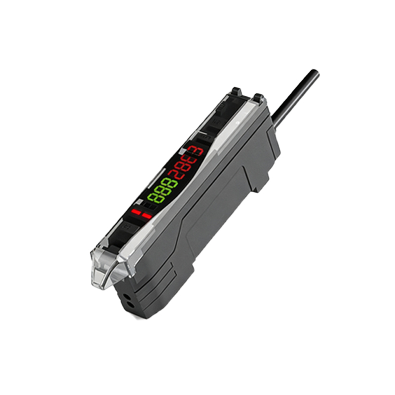
The Electromagnetic Spectrum in Sensing: Key Ranges
A typical wavelength range diagram highlights three primary bands: visible light (400-700 nm), near-infrared (NIR, 700-1000 nm), and short-wave infrared (SWIR, 1000-3000 nm). Infrared sensors, often operating at 850 nm or 940 nm, are common in industrial applications due to their immunity to visible ambient light and ability to penetrate thin fog or dust. Visible red light (660 nm) is used in precision tasks like label detection, offering better alignment with human visual inspection. Engineers must note that the sensor’s effective range—often measured in meters—declines as wavelength increases due to absorption in certain materials, such as water vapor in SWIR bands.
Reading a Wavelength Range Diagram: Axes and Curves
The diagram typically plots wavelength (nm) on the x-axis versus relative sensitivity or transmittance (%) on the y-axis. A peak curve indicates the sensor’s maximum response at a specific wavelength, while flanking slopes show reduced performance. For example, a photoelectric sensor with a peak at 880 nm may have a usable range of 800-950 nm, with sensitivity dropping below 50% at the edges. Engineers should also examine the detector’s spectral response curve, which accounts for the photodiode or phototransistor’s material properties (e.g., silicon for NIR, InGaAs for SWIR). This data helps in matching the sensor to the target object’s reflectivity—dark objects absorb more light, requiring higher sensitivity in the chosen band.
Practical Impact of Wavelength on Detection Reliability
Selecting the wrong wavelength range can lead to missed detections or false positives in industrial settings. For instance, a sensor using 650 nm visible light may struggle with transparent glass or glossy surfaces due to specular reflections, while an 850 nm NIR sensor performs better on such materials by penetrating surface glare. Additionally, in environments with high ambient light (e.g., near welding or solar exposure), sensors operating in the SWIR range (1550 nm) are preferred because they are less affected by sunlight interference. Wavelength range diagrams also show how temperature variations shift the peak wavelength—a critical factor for sensors in ovens or cold storage facilities.
Interpreting Multi-Wavelength Diagrams for Advanced Sensors
Some industrial photoelectric sensors use multi-wavelength emission (e.g., dual-beam or color sensors) to distinguish between object types. Their range diagrams show multiple peaks, each corresponding to a different LED or laser source. For example, a color sensor might use red (630 nm), green (520 nm), and blue (470 nm) to detect packaging labels. Engineers must analyze how the relative intensities of these peaks change with distance, as the sensor’s optics (lenses or fiber optics) can introduce chromatic aberration. Calibration curves in the diagram help correct for this, ensuring consistent detection across the full sensing range.
Conclusion: Leveraging Wavelength Data for Robust Design
Mastering photoelectric sensor wavelength range diagrams empowers engineers to optimize system design by reducing installation costs and minimizing maintenance. By correlating the diagram with factors like object color, surface texture, and environmental interference, professionals can avoid common pitfalls such as sensor blinding or range loss. Always reference the manufacturer’s datasheet for exact wavelength tolerances and test under real-world conditions (e.g., using a spectrometer to verify output). With this knowledge, industries can achieve higher throughput and lower downtime in automated processes.