Introduction to Photoelectric Sensing Fundamentals
At its core, a photoelectric sensor operates on the principle of converting light signals into electrical signals to detect the presence, absence, or distance of an object. The fundamental components of any photoelectric sensor system include a light source (emitter), a photodetector (receiver), and associated signal processing circuitry. The emitter, typically a Light Emitting Diode (LED) or a laser diode, projects a beam of light. The receiver, which can be a phototransistor, photodiode, or photoelectric cell, is positioned to receive this light under normal, unobstructed conditions. When an object interrupts or reflects this light beam, it causes a measurable change in the electrical output of the receiver. This change is then processed by the sensor's internal electronics to generate a discrete on/off signal or an analog output proportional to distance or light intensity. Understanding this basic light-to-electricity conversion is the first step in deciphering any photoelectric sensor schematic.
Deciphering the Emitter Circuit Schematic
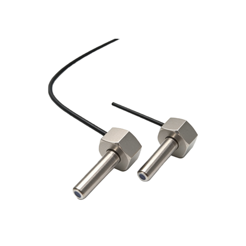
The emitter section of a photoelectric sensor schematic is dedicated to generating a stable and consistent light beam. A typical circuit will feature the light-emitting component (LED/Laser Diode) as its central element. This component is driven by a constant current source circuit to ensure luminous intensity remains unaffected by voltage fluctuations or temperature variations. The schematic will show the LED in series with a current-limiting resistor, but more advanced designs incorporate operational amplifiers or dedicated driver ICs to precisely control the current. For modulated light types (common to avoid ambient light interference), an oscillator circuit is integrated. This oscillator, often built around a 555 timer IC or a microcontroller, switches the LED on and off at a specific high frequency (e.g., 1-10 kHz). The schematic will depict the connections between the oscillator output, the driver stage, and the LED. Power supply filtering capacitors and protection diodes (like a flyback diode for inductive loads) are also standard schematic symbols found in this section to ensure clean, reliable operation.
Analyzing the Receiver and Amplification Stage
The receiver circuit is responsible for detecting the faint light signal and converting it into a usable electrical voltage. The photodetector (e.g., phototransistor) is the key symbol here, often shown with its collector and emitter terminals. In a schematic, the photodetector is usually configured in a common-emitter amplifier setup. The incident light generates a small base current, which is amplified to produce a larger collector current. This raw signal is extremely small and noisy. Therefore, the next critical stage is the signal amplifier. Schematics will detail one or more operational amplifier (op-amp) stages configured as transimpedance amplifiers (converting current to voltage) or non-inverting amplifiers. Key components around the op-amps include feedback resistors to set gain and capacitors to filter out unwanted high-frequency noise or to form band-pass filters that only allow the sensor's specific modulation frequency to pass, effectively rejecting ambient light.
Signal Processing and Output Circuitry
After amplification, the signal enters the processing stage. For modulated sensors, this involves a demodulator circuit. The schematic for this section might show a mixer or a synchronous detector that compares the received modulated signal with the original modulation frequency from the emitter oscillator, extracting the true signal. This is followed by a comparator circuit. The comparator, another op-amp or a dedicated comparator IC, compares the processed signal voltage against a preset reference voltage (threshold). This reference is often adjustable via a potentiometer shown on the schematic, allowing sensitivity adjustment. When the signal exceeds the threshold, the comparator's output switches state (e.g., from low to high). This clean digital signal then feeds into the output stage. The output stage schematic shows the final switching element, such as an NPN/PNP transistor, a MOSFET, or a relay driver IC, which interfaces with the external load (PLC, relay, etc.). Protection components like clamping diodes and current-limiting resistors are always present around the output transistor.
Power Supply and Integration in the Complete Schematic
No sensor operates without a stable power source. The power supply section of the schematic is crucial for overall reliability. It typically shows a voltage regulator IC (like a 78xx series or a low-dropout regulator) that converts the incoming supply voltage (e.g., 12-24V DC) to the stable lower voltages (e.g., 5V, 3.3V) required by the oscillator, op-amps, and logic circuits. The schematic details input and output filtering capacitors to smooth out voltage ripples and suppress electrical noise. Transient voltage suppression (TVS) diodes or varistors may be included to protect against voltage spikes. A complete system schematic integrates all these blocks—power supply, emitter, receiver, amplifier, processor, and output—showing their interconnections. Reading such a schematic from left to right generally follows the signal flow: power in, light generation, light detection, signal conditioning, decision making, and finally, switched output. Understanding each block's function allows engineers to troubleshoot, customize, or integrate the sensor effectively into larger automation systems.