Introduction to Photoelectric Sensor PIN Technology
The photoelectric sensor PIN, a cornerstone of modern industrial automation, represents a critical evolution in optical sensing technology. At its core, a PIN photodiode is a specific type of semiconductor photodetector that converts light into an electrical current. The acronym "PIN" refers to its distinct layered structure: a P-type layer, an Intrinsic (or undoped) layer, and an N-type layer. This intrinsic region is the key differentiator from standard PN photodiodes. It is significantly wider, which reduces the junction capacitance and allows the device to operate at much higher speeds and with greater sensitivity, particularly to low-light conditions. This makes the PIN photodiode exceptionally well-suited for the demanding environments and precise requirements of industrial photoelectric sensors, where rapid detection and reliable signal generation are paramount.
Core Operating Principles and Structure
Understanding the operational mechanics of a PIN photodiode is essential for optimal sensor design and application. When photons of sufficient energy strike the photodiode, they are absorbed within the semiconductor material, primarily in the intrinsic region. This absorption generates electron-hole pairs. The wide intrinsic region, under the influence of the built-in electric field (often enhanced by an external reverse bias voltage), allows these charge carriers to drift rapidly across the junction. This movement constitutes a photocurrent that is directly proportional to the intensity of the incident light. The reverse bias voltage serves a dual purpose: it widens the depletion region, effectively extending the intrinsic layer for better charge collection, and it accelerates the carrier drift velocity, thereby improving the sensor's response time. This fundamental principle enables photoelectric sensors to detect the presence, absence, or distance of an object by interpreting changes in this generated photocurrent.
Key Advantages in Industrial Sensing Applications
The integration of PIN photodiodes into photoelectric sensors confers several decisive advantages in industrial settings. First and foremost is their high-speed response. The low junction capacitance enables switching frequencies in the megahertz range, allowing for the detection of very fast-moving objects on high-speed production lines. Secondly, their superior linearity and wide dynamic range make them ideal for analog sensing applications, such as precise positioning or contrast detection, where the output signal must accurately reflect subtle variations in light intensity. Furthermore, PIN photodiodes exhibit excellent temperature stability compared to other photodetectors like phototransistors, leading to more consistent performance across varying environmental conditions on the factory floor. Their robustness and reliability under continuous operation solidify their status as the detector of choice for diffuse, retro-reflective, and through-beam sensor configurations.
Critical Selection Parameters for System Design
Selecting the appropriate PIN photodiode for a specific photoelectric sensor requires careful consideration of several technical parameters. Responsivity, measured in amperes per watt (A/W), indicates how effectively the device converts optical power into electrical current; it is wavelength-dependent and must be matched to the light source, typically an infrared or visible LED or laser diode. Dark current, the small current that flows even in the absence of light, is a source of noise and should be minimized, especially in low-light sensing. The active area size of the diode affects sensitivity and should be chosen based on the optical design and required sensing spot size. Additionally, parameters like rise/fall time, terminal capacitance, and spectral response range must be evaluated against the application's required sensing speed, bandwidth, and environmental light conditions. Proper optical design, including lenses and filters, is also crucial to maximize signal-to-noise ratio.
Common Applications Across Automation Sectors
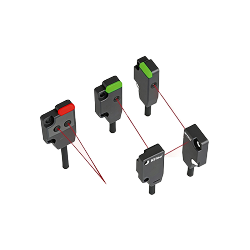
Photoelectric sensors utilizing PIN technology are ubiquitous in automation. In material handling, they count, sort, and detect the position of boxes on conveyors. In packaging machinery, they ensure precise label registration, fill-level control, and tamper-evident seal verification. Automotive assembly lines rely on them for robot guidance, part verification, and weld seam tracking. Their high speed is exploited in printing and paper processing for web break detection and registration mark reading. Furthermore, in cleanroom and electronic assembly environments, they perform non-contact object detection without risking contamination or damage to delicate components. The versatility of the through-beam, retro-reflective, and diffuse sensing modes, all enabled by the reliable PIN detector, allows solutions for nearly every object detection challenge.
Integration and Circuit Considerations
Effectively integrating a PIN photodiode into a sensor circuit demands attention to signal conditioning. Due to the typically low-level photocurrent output, a transimpedance amplifier (TIA) is almost always employed to convert this current into a usable voltage signal. The design of this amplifier is critical: feedback resistor and capacitor values must be chosen to provide sufficient gain while managing bandwidth and stability, preventing oscillation. Shielding and proper PCB layout are mandatory to mitigate electromagnetic interference (EMI), which can easily swamp the tiny photocurrent signal. For digital output sensors, a comparator stage follows the TIA to create a clean switching signal. For analog or distance-measuring sensors, the amplified voltage is processed directly. Power supply decoupling and protection against voltage transients are also essential for ensuring long-term reliability in harsh industrial environments.
Future Trends and Developments
The future of PIN-based photoelectric sensing is aligned with broader Industry 4.0 trends. We are witnessing a push towards miniaturization, enabling smaller sensor housings for installation in tight spaces. There is also a growing demand for sensors with integrated intelligence, such as IO-Link communication, which allows for parameter setting, condition monitoring, and diagnostic data reporting directly from the sensor's PIN detector and processing circuitry. Enhanced background suppression capabilities through advanced optical designs and signal processing algorithms continue to improve. Furthermore, the development of PIN photodiodes on new semiconductor materials may expand the usable spectral range and improve performance characteristics, ensuring this foundational technology remains vital for next-generation smart factories and automated systems.