Understanding Photoelectric Sensor Components
Photoelectric sensors are fundamental devices in industrial automation, relying on precise components to function. A typical sensor comprises several key parts: the emitter, receiver, housing, lens, and electrical connectors. The emitter, usually an LED or laser diode, generates the light beam. The receiver, a phototransistor or photodiode, detects the presence or absence of this beam. The housing, often made of durable plastic or metal, protects the internal electronics from environmental factors like dust, moisture, and mechanical impact. The lens focuses the emitted light and enhances the receiver's sensitivity. Understanding each component's specifications, such as the emitter's wavelength and the receiver's response time, is crucial for selecting the right sensor for an application. Detailed part drawings provide exact dimensions, material grades, and tolerance levels for manufacturing and replacement purposes.
Interpreting Part Drawings for Key Elements
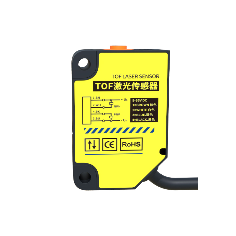
Part drawings, or detail drawings, are essential technical documents. For a photoelectric sensor's emitter module, the drawing will specify critical dimensions: the diameter and focal length of the lens, the precise positioning of the LED chip, and the pin configuration for the electrical leads. Tolerances, often indicated with geometric dimensioning and tolerancing (GD&T) symbols, ensure the component fits and functions within the assembly. Surface finish requirements might be noted for the lens to minimize light diffusion. Material callouts, such as "Polycarbonate for lens" or "Stainless Steel 316 for housing," are vital for durability and optical clarity. Engineers must cross-reference these drawings with the bill of materials (BOM) to verify part numbers and sourcing information during procurement or troubleshooting.
The Role of Assembly Drawings in System Integration
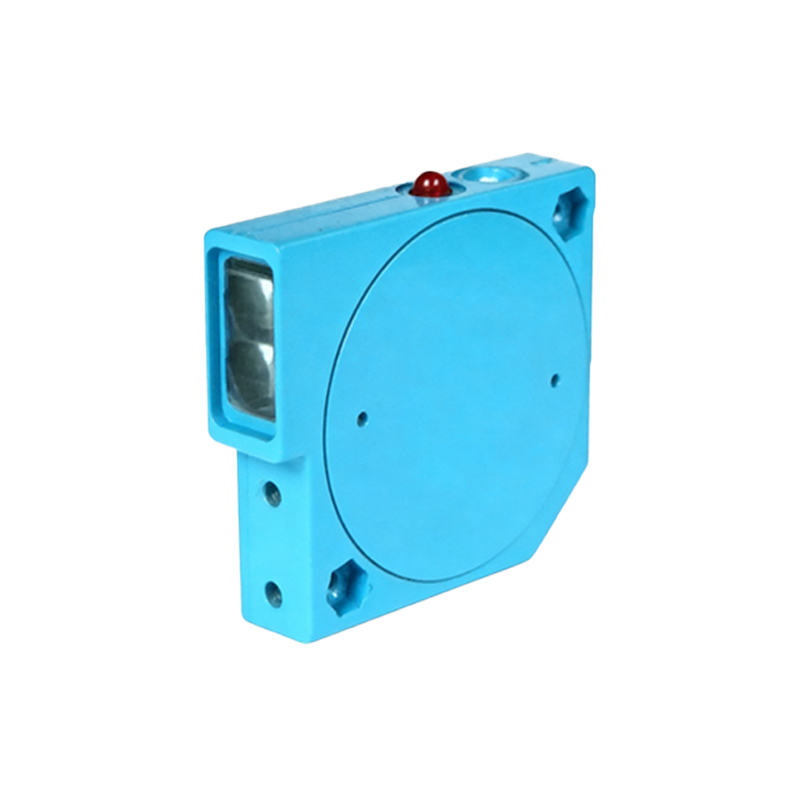
Assembly drawings illustrate how all individual parts come together to form a complete photoelectric sensor unit. These drawings show the spatial relationship between the emitter, receiver, PCB (printed circuit board), housing shells, and cable gland. Exploded-view assembly drawings are particularly useful, displaying components slightly separated along an axis, which clarifies the order of assembly. Key features include section views that reveal internal layouts and callouts with leader lines pointing to sub-assembly groups. Assembly drawings also specify fastening methods, such as the type and torque specifications for screws used to seal the housing. This documentation is indispensable for maintenance technicians during disassembly and reassembly, ensuring correct alignment and preventing damage to sensitive optical elements.
Critical Dimensions and Tolerances in Alignment
The performance of a photoelectric sensor heavily depends on the precise alignment of the emitter and receiver. Assembly drawings define the critical alignment dimensions, such as the coaxiality between the emitter lens and the receiver lens or their parallel offset in a retro-reflective sensor model. Tolerances on these dimensions are extremely tight, sometimes within a few microns, to ensure the light beam is accurately projected and detected. Drawings may include datum references and control frames from GD&T to specify these alignment requirements unambiguously. Ignoring these tolerances during assembly or mounting can lead to reduced sensing range, false triggers, or complete operational failure. Therefore, manufacturers provide detailed mounting hole patterns and alignment guides within the assembly drawing set.
Electrical Interface and Wiring Diagrams
Beyond mechanical assembly, photoelectric sensors require correct electrical integration. Assembly drawing packages often include wiring diagrams or schematic inserts. These diagrams detail the connections between the sensor's PCB and its external cable or connector. They specify wire colors, gauge, terminal block positions, and pin assignments for output types (e.g., NPN, PNP, or analog). For sensors with built-in amplifiers or programmable logic, the drawing might show DIP switch settings or indicator LED locations. This information ensures proper interface with PLCs (Programmable Logic Controllers) and other control systems, preventing issues like reverse polarity or signal short circuits that could damage the sensor.
Best Practices for Using These Drawings
Effective utilization of part and assembly drawings streamlines the entire lifecycle of a photoelectric sensor. During design-in, engineers use them to verify form, fit, and function within a machine layout. For procurement, accurate part numbers from drawings prevent ordering errors. On the production floor, assembly drawings guide technicians in building and testing sensor units. In the field, maintenance personnel rely on exploded views and part lists for efficient repair. It is a best practice to always use the most recent revision of a drawing, as indicated in the title block, and to understand all notes and symbols in the legend. Digital management of these drawings in PDF or CAD formats facilitates easy sharing and reference across engineering, manufacturing, and service teams.