Introduction to Photoelectric Sensor Fabrication
The fabrication of photoelectric sensors represents a critical intersection of materials science, semiconductor physics, and precision engineering. These devices, which convert light signals into electrical signals, are foundational components in automation, safety systems, and countless industrial applications. The core principle involves the photoelectric effect, where incident photons with sufficient energy liberate electrons within a photosensitive material, generating a measurable current or voltage change. The choice of fabrication method directly influences key sensor parameters such as responsivity, spectral range, response time, dark current, and long-term stability. Engineers must select a fabrication pathway that aligns with the target application's requirements for sensitivity, environmental robustness, cost, and form factor. This guide delves into the primary methodologies employed in modern photoelectric sensor manufacturing, outlining their processes, material considerations, and typical use cases.
Semiconductor-Based Fabrication Techniques
Semiconductor processes form the backbone of most commercial photoelectric sensor production, particularly for photodiodes, phototransistors, and charge-coupled devices (CCDs). The journey begins with a high-purity semiconductor wafer, typically silicon (Si) for visible and near-infrared light, or specialized materials like indium gallium arsenide (InGaAs) for infrared detection. The fabrication involves a series of sophisticated steps performed in cleanroom environments. Photolithography is used to define intricate patterns on the wafer surface. Subsequent doping processes, such as ion implantation or diffusion, create the essential p-n junctions or PIN structures that form the active region of the sensor. Chemical vapor deposition (CVD) and physical vapor deposition (PVD) are employed to deposit thin films for passivation layers, anti-reflective coatings, and electrical contacts. Finally, the wafer is diced into individual sensor chips, which are then packaged with a transparent window or lens. This method offers exceptional consistency, high-volume scalability, and excellent performance characteristics, making it ideal for consumer electronics, industrial automation sensors, and imaging arrays.
Thin-Film and Deposition Methods
For applications requiring large-area sensors, flexibility, or sensitivity to specific wavelengths not covered by traditional semiconductors, thin-film fabrication techniques are paramount. These methods involve depositing photosensitive layers onto a substrate, which can be glass, plastic, or even metal. Common materials include amorphous silicon (a-Si), organic photodetectors (OPDs), and perovskite compounds. Techniques like sputtering, thermal evaporation, and spin-coating are utilized to create uniform thin films. A key advantage is the ability to create multi-layer structures, such as tandem cells or heterojunctions, which can broaden the spectral response or improve quantum efficiency. Furthermore, these processes can be adapted for roll-to-roll manufacturing, significantly reducing cost for large-area applications like scanner beds, touchless panels, and some biomedical sensors. However, thin-film sensors often exhibit slower response times and higher noise compared to their crystalline semiconductor counterparts, necessitating careful design trade-offs.
Hybrid and Integrated Fabrication Approaches
Advanced sensor systems often demand performance beyond the scope of a single material or process. Hybrid fabrication addresses this by combining different technologies into a single package. A prime example is the hybridization of a silicon readout integrated circuit (ROIC) with a mercury cadmium telluride (HgCdTe) or quantum dot infrared photodetector (QDIP) array for high-performance thermal imaging. This typically involves flip-chip bonding, where the detector array is precisely aligned and connected to the ROIC via micro-bumps. Another integrated approach is the monolithic integration of photodetectors with signal conditioning circuitry (amplifiers, analog-to-digital converters) on the same silicon chip using standard complementary metal-oxide-semiconductor (CMOS) or bipolar-CMOS (BiCMOS) processes. This results in highly compact, low-power, and intelligent "sensor-on-a-chip" solutions crucial for portable devices, automotive LiDAR, and advanced optical communication modules.
Packaging and Environmental Protection
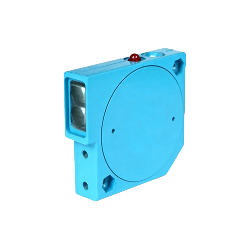
The fabrication process is not complete without robust packaging, which protects the delicate semiconductor die from mechanical stress, moisture, dust, and chemical contamination. Packaging also provides the necessary electrical connections and optical interface. For photoelectric sensors, the package must include a transparent or wavelength-specific window, often made of glass, epoxy, or sapphire. Hermetic sealing using metal or ceramic packages is essential for sensors deployed in harsh environments or requiring extreme long-term reliability. The design of the package also influences the sensor's field of view and optical characteristics. Engineers must consider factors like window transmittance, internal reflections, and the potential for condensation. Effective packaging is as critical as the chip fabrication itself in determining the final product's performance, durability, and suitability for field deployment in industrial, automotive, or outdoor settings.
Testing, Calibration, and Quality Assurance
Post-fabrication, every photoelectric sensor undergoes rigorous testing and calibration to ensure it meets specified performance criteria. Standard tests include measuring spectral responsivity (output per unit of optical power at different wavelengths), linearity (output versus input light intensity), response time (rise and fall times), and noise-equivalent power (NEP). Dark current, the current that flows in the absence of light, is a critical parameter that affects the sensor's low-light sensitivity and must be minimized. Calibration involves exposing the sensor to known light sources and adjusting output signals to a standard scale. Environmental stress testing, such as temperature cycling, humidity exposure, and vibration tests, validates the sensor's reliability. A comprehensive quality assurance protocol, often involving statistical process control (SPC) during fabrication and final automated optical inspection (AOI), is indispensable for delivering consistent, high-quality sensors to the market.