Introduction to Photoelectric Sensors
Photoelectric sensors are indispensable components in modern industrial automation, enabling non-contact detection of objects through the use of light beams. These sensors are widely employed across various sectors, including manufacturing, packaging, and material handling, due to their high precision, reliability, and versatility. The core principle involves emitting a light beam—typically infrared, visible, or laser—and detecting changes in the received light caused by the presence, absence, or characteristics of a target object. This technology allows for rapid and accurate sensing in challenging environments where physical contact is impractical or undesirable. The manufacturing of these sensors requires meticulous attention to detail, integrating optical, electronic, and mechanical engineering to ensure consistent performance under industrial conditions. As automation advances, the demand for robust and efficient photoelectric sensors continues to grow, driving innovations in their design and production processes.
Design and Engineering Phase
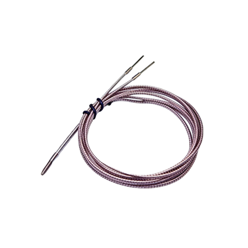
The manufacturing journey begins with a comprehensive design and engineering phase, where specifications are defined based on application requirements. Engineers collaborate to select appropriate light sources, such as LEDs or laser diodes, and photodetectors, like phototransistors or photodiodes, considering factors like detection range, response time, and environmental resilience. Circuit design focuses on signal processing, incorporating amplifiers, filters, and output modules to convert light variations into electrical signals. Mechanical housing is also designed to provide protection against dust, moisture, and mechanical shocks, often adhering to IP ratings for industrial use. Prototyping follows, involving simulations and initial builds to validate functionality. This stage ensures that the sensor meets performance benchmarks, such as sensing distance and accuracy, before moving to mass production. Iterative testing refines the design, addressing any issues related to interference or durability.
Component Sourcing and Preparation
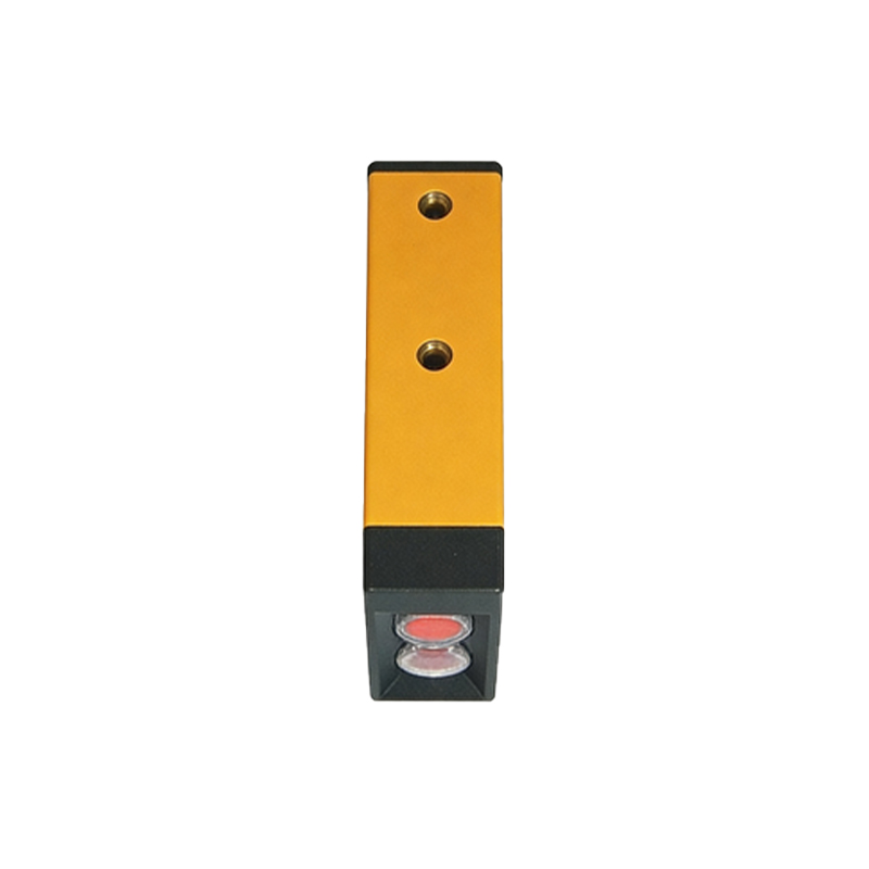
High-quality components are critical for reliable sensor performance. Sourcing involves procuring optical elements, electronic chips, connectors, and housing materials from certified suppliers. LEDs and photodetectors undergo rigorous inspection to verify wavelength consistency and sensitivity. Electronic components, including microcontrollers and resistors, are tested for compliance with industry standards. The housing, typically made from durable plastics or metals, is prepared through molding or machining processes to achieve precise dimensions. All parts are cleaned and prepared for assembly in a controlled environment to prevent contamination. This step emphasizes supply chain management to ensure consistency and avoid delays, as any defect in components can compromise the final product's functionality. Inventory is tracked meticulously to support efficient production flow.
Assembly Process Overview
Assembly is conducted in a cleanroom or controlled setting to minimize dust and static interference. The process starts with mounting the light source and photodetector onto a printed circuit board (PCB) using automated pick-and-place machines. Soldering, often via reflow or wave techniques, secures these components, followed by optical alignment to ensure the emitted and received beams are accurately positioned. Lenses or filters may be added to focus or filter light, enhancing detection capabilities. The assembled PCB is then integrated into the housing, with seals applied for environmental protection. Connectors and cables are attached for power and signal transmission. Each assembly station includes quality checks, such as visual inspections and functional tests, to identify any misalignments or defects early. This streamlined approach ensures efficiency while maintaining high standards.
Calibration and Testing Procedures
Calibration is essential to guarantee sensor accuracy and reliability. After assembly, each unit undergoes calibration using standardized targets at specified distances. Equipment adjusts sensitivity thresholds to match design specifications, ensuring consistent output signals. Testing follows, involving multiple scenarios: detection range verification, response time measurement, and environmental stress tests. Sensors are exposed to variations in temperature, humidity, and vibration to simulate industrial conditions. Electrical tests check for proper voltage levels and output types (e.g., NPN/PNP). Advanced systems may include automated optical inspections and signal analysis. Any unit failing these tests is flagged for rework or rejection. This rigorous phase ensures that only sensors meeting strict performance criteria proceed to packaging, reducing field failures and enhancing customer trust.
Quality Assurance and Final Inspection
Quality assurance permeates the entire manufacturing process, with final inspection serving as the last checkpoint. Inspectors review the sensor's physical integrity, verifying housing seals and connector stability. Functional tests repeat key performance metrics, such as detection consistency under different lighting conditions. Documentation, including calibration certificates and compliance labels (e.g., CE, RoHS), is prepared for each batch. Statistical process control methods monitor production trends, identifying potential improvements. Samples from each lot may undergo accelerated life testing to predict longevity. Once approved, sensors are cleared for packaging. This stage emphasizes traceability, with serial numbers logged for future reference. By adhering to international quality standards, manufacturers ensure that photoelectric sensors deliver dependable operation in diverse industrial applications.
Packaging and Distribution
Packaging protects sensors during transit and storage while providing essential information. Units are placed in anti-static bags or cushioned containers to prevent damage from shocks or electrostatic discharge. Labels include model numbers, specifications, and handling instructions. Bulk packaging for industrial clients often involves cartons or pallets optimized for logistics. Distribution channels are coordinated to meet global demand, with inventory managed through enterprise resource planning systems. Manufacturers may offer customization, such as adding mounting brackets or cables, based on client needs. Before shipment, a final audit confirms order accuracy and packaging integrity. Efficient distribution ensures timely delivery to end-users, supporting seamless integration into automation systems. Post-sale, technical support and documentation aid in installation and maintenance, fostering long-term reliability.
Conclusion and Industry Trends
The manufacturing of industrial photoelectric sensors is a complex, multi-stage process that blends precision engineering with stringent quality control. From design to distribution, each step aims to produce durable, high-performance sensors capable of withstanding harsh industrial environments. Emerging trends, such as the integration of IoT connectivity and smart sensors with self-diagnostic features, are shaping future production methods. Advances in miniaturization and energy efficiency also drive innovation, allowing for more compact and sustainable designs. As industries increasingly adopt automation, the role of photoelectric sensors will expand, necessitating continuous improvement in manufacturing techniques. By focusing on reliability and adaptability, manufacturers can meet evolving demands, contributing to safer and more efficient industrial operations worldwide.