Introduction to Thin-Film Photoelectric Sensor Technology
Thin-film photoelectric sensors represent a significant advancement in optical sensing technology, widely adopted across industrial automation. Unlike traditional bulky sensors, these devices utilize sophisticated thin-film deposition techniques to create ultra-compact, highly sensitive photodetectors and often integrated light sources on a single substrate. The core principle involves the photoelectric effect, where light incident on a thin semiconductor layer—such as amorphous silicon, cadmium sulfide, or organic photoconductive materials—generates an electrical signal. This signal change is then processed by onboard electronics to detect the presence, absence, or specific characteristics of an object. The thin-film construction not only minimizes the sensor's footprint but also enhances its response speed, durability, and consistency, making it ideal for high-precision applications in constrained spaces.
Key Operational Modes and Sensing Methodologies
These sensors primarily operate in three fundamental modes: through-beam, retro-reflective, and diffuse reflective. In the through-beam mode, the emitter and receiver are separate units. An object is detected when it interrupts the light beam traveling from the emitter to the receiver, offering the longest sensing range and highest reliability. The retro-reflective mode positions the emitter and receiver in the same housing, using a reflector to bounce the light beam back. Detection occurs when the beam is blocked. This mode simplifies alignment. The most common for thin-film sensors is the diffuse reflective mode, where the emitted light reflects off the target object itself back to the receiver. Advanced versions incorporate background suppression or fixed-field teaching, allowing them to ignore distant backgrounds and detect objects only within a precise, predefined range, which is crucial for handling varied surface colors and reflectivities.
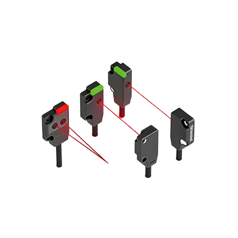
Advantages Over Conventional Photoelectric Sensors
The transition to thin-film technology confers several compelling advantages. First is the remarkable miniaturization, enabling installation in extremely tight locations on modern machinery and robotic arms. Second, the manufacturing process allows for excellent batch-to-bin consistency and long-term stability, as the thin-film layers are less prone to degradation compared to discrete components. Third, they often exhibit lower power consumption, which is beneficial for portable or battery-operated systems. Furthermore, the integrated design reduces susceptibility to vibration and misalignment. The protective coating on the thin-film element can be tailored for resistance to dust, moisture, and certain chemicals, significantly enhancing the sensor's lifespan and reliability in harsh industrial environments like packaging, material handling, and automotive assembly lines.
Primary Industrial Applications and Use Cases
Thin-film photoelectric sensors are ubiquitous in automation. In electronics manufacturing, they are indispensable for verifying component placement on PCBs, counting tiny parts, and detecting tape-and-reel packaging positions. Within the pharmaceutical and packaging industries, they ensure precise label registration, verify cap placement on bottles, and detect transparent films or missing products in blister packs. Automated assembly lines use them for robotic guidance, checking for part presence in fixtures, and precise positioning control. Their ability to detect small, fast-moving, or low-contrast objects makes them perfect for print registration in textile and printing machinery. Additionally, they are increasingly used in consumer devices for touchless interfaces and position feedback due to their slim profile.
Critical Factors for Sensor Selection and Integration
Selecting the appropriate thin-film photoelectric sensor requires careful analysis of the application parameters. The sensing distance, determined by the mode and the target's reflectivity, is paramount. The size, color, material, and surface finish of the target object directly influence the choice of sensor type; a background suppression diffuse sensor is often necessary for inconsistent targets. Environmental conditions such as ambient light (requiring modulated LED light sources to prevent interference), temperature extremes, and exposure to contaminants dictate the required ingress protection (IP) rating and housing material. Electrical output type (PNP/NPN, analog, or IO-Link for smart sensing), supply voltage compatibility, and response speed must align with the control system's requirements. Proper mounting, alignment, and routine maintenance of the lens surface are also crucial for sustained optimal performance.
Future Trends and Technological Evolution
The future of thin-film photoelectric sensing is geared towards greater intelligence, connectivity, and versatility. The integration of IO-Link communication protocol is becoming standard, enabling sensors to transmit detailed diagnostic data, parameter settings, and process values to higher-level control systems for predictive maintenance and Industry 4.0 analytics. Advancements in materials science may lead to sensors capable of operating in wider spectral ranges (e.g., UV or IR) for specialized detection tasks. There is also a trend towards multi-functional sensors that combine photoelectric sensing with measurement of distance, color, or contrast in a single, ultra-thin package. As machinery continues to shrink and demand for precision grows, the role of these robust, miniature sensors will only expand, driving further innovation in their design and application capabilities.