The Dawn of Photoelectric Sensing
The story of photoelectric sensors begins not on the factory floor, but in the realm of fundamental physics. The foundational principle, the photoelectric effect, was first rigorously explained by Albert Einstein in 1905, for which he later received the Nobel Prize. This discovery—that light incident upon a material can liberate electrons—laid the theoretical groundwork. Early applications were limited to laboratory settings and rudimentary light detectors. The first commercially viable devices emerged in the mid-20th century, utilizing simple vacuum tube photodetectors. These early sensors were bulky, fragile, required high operating voltages, and were sensitive only to specific light spectra. Their industrial use was minimal, confined to basic counting tasks or as safety interlocks where reliability was less critical. The core components—an emitter (often an incandescent bulb) and a receiver (a phototube)—defined the basic through-beam principle that remains a cornerstone today, albeit in a vastly more sophisticated form.
The Solid-State Revolution
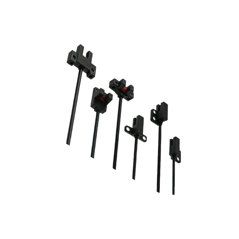
The invention of the transistor and subsequent advancements in semiconductor technology in the 1960s and 70s catalyzed the first major leap in photoelectric sensor development. The introduction of light-emitting diodes (LEDs) as reliable, long-lasting light sources replaced fragile incandescent bulbs. Simultaneously, phototransistors and photodiodes emerged as compact, efficient, and robust receivers. This solid-state revolution dramatically reduced sensor size, power consumption, and heat generation while improving switching speeds and lifespan. Engineers could now package the emitter and receiver into smaller housings, enabling the proliferation of diffuse-reflective sensors, where the sensor houses both elements and detects light reflected from the target itself. This eliminated the need for a separate reflector or receiver unit, simplifying installation for a vast array of applications, from object detection on conveyors to bottle cap presence verification.
Integration and Intelligence
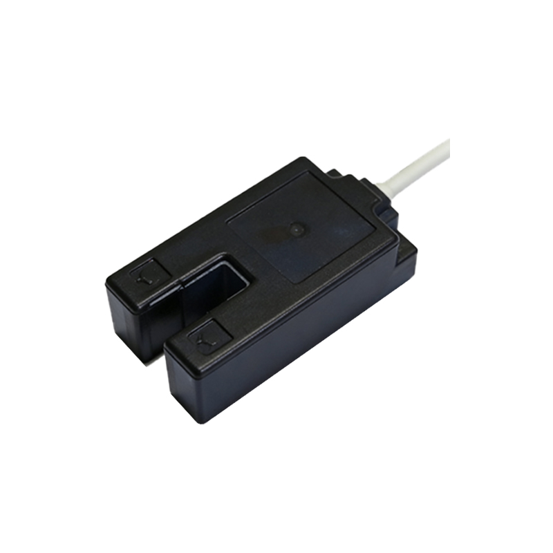
The 1980s and 90s saw the integration of microprocessors and application-specific integrated circuits (ASICs) into sensor design. This marked the transition from purely analog devices to "smart" sensors with embedded logic. Background suppression technology was a key innovation, using triangulation principles to detect an object only within a precise, programmable distance window, ignoring objects and backgrounds beyond it. This solved persistent problems with diffuse sensors detecting conveyor belts or machine parts behind the target. Furthermore, modulated LED light (typically in the infrared or visible red spectrum) became standard. By pulsing the LED at a high frequency and tuning the receiver to that specific frequency, sensors gained immense immunity to ambient light interference from factory lighting, sunlight, or other sources, vastly improving reliability in harsh industrial environments.
The Era of Specialization and Connectivity
From the 2000s onward, development has focused on extreme specialization, miniaturization, and connectivity. Laser-based sensors offer micrometer-level precision for positioning and inspection tasks. Fiber optic sensors, using flexible light guides, allow sensing in extremely hot, cold, or space-constrained environments where the electronics cannot be placed. Color sensors, contrast sensors, and luminescence sensors address complex quality control needs. The housing materials evolved to include robust metals and chemically-resistant polymers for washdown (IP69K) applications in food and pharmaceutical industries. Most recently, the integration of Industrial Internet of Things (IIoT) capabilities has become a frontier. Modern sensors feature IO-Link communication, providing detailed diagnostic data (like lens contamination levels, signal strength, and operating temperature) directly to the control system, enabling predictive maintenance and seamless integration into Industry 4.0 architectures.
Modern Design and Future Trajectories
Today's photoelectric sensor is a marvel of integrated engineering. A typical cross-section reveals a precision-molded housing, a high-output LED or laser diode, a lens system for beam shaping and focus, a high-sensitivity photodiode array, a powerful ASIC for signal processing and modulation, and robust amplification circuitry. Advanced models incorporate teach-in functions via pushbuttons or remote signals, allowing for quick setup without tools. Looking forward, development is geared towards even smaller form factors, increased sensing ranges, and enhanced data intelligence. The convergence of sensing and vision technology is ongoing, with "smart sensors" capable of simple shape recognition or measurement. Furthermore, the use of new light spectra and advanced algorithms continues to push the boundaries of what can be detected—from transparent films and clear glass to specific chemical compositions—ensuring photoelectric sensors remain indispensable in the automated world.