Introduction to Radiation-Hardened Photoelectric Sensors
Photoelectric sensors are fundamental components in automation and control systems, converting light signals into electrical outputs. However, in environments with high levels of ionizing radiation—such as nuclear power plants, space applications, particle accelerators, and certain medical equipment—standard sensors can fail catastrophically. Radiation can induce transient faults, degrade performance over time, or cause permanent damage through mechanisms like Single Event Upsets (SEUs), latch-up, and total ionizing dose (TID) effects. A radiation-hardened (rad-hard) photoelectric sensor is specifically engineered to withstand these harsh conditions. Its schematic design is not merely a robust version of a standard sensor; it incorporates specialized components, layout techniques, and redundancy to ensure reliable operation where failure is not an option. The core principle involves shielding critical elements, selecting inherently radiation-tolerant materials and semiconductors, and designing circuits that can tolerate or correct errors induced by radiation.
Core Components and Their Rad-Hard Characteristics
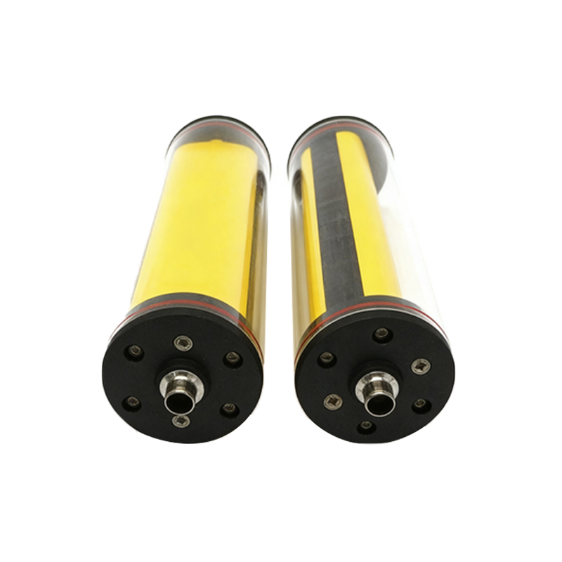
The schematic of a rad-hard photoelectric sensor revolves around several key components, each chosen or designed for radiation tolerance. The photodetector itself, often a photodiode or phototransistor, is critical. In rad-hard designs, designers frequently prefer PIN photodiodes made from wide-bandgap semiconductors like silicon carbide (SiC) or gallium nitride (GaN). These materials have a higher displacement energy threshold, making them less susceptible to radiation-induced lattice damage. The schematic symbol remains the same, but the material specification is paramount. Following the detector, the amplification stage is vulnerable. Rad-hard operational amplifiers and comparators are used, which are fabricated using Silicon-on-Insulator (SOI) or specialized bipolar-CMOS processes that mitigate latch-up and reduce charge collection volumes. Passive components are also selected carefully; thin-film resistors are preferred over thick-film for better stability under TID, and ceramic capacitors with specific dielectrics (like NP0/C0G) are chosen for their minimal parametric shift.
Schematic Design for Mitigating Single Event Effects (SEE)
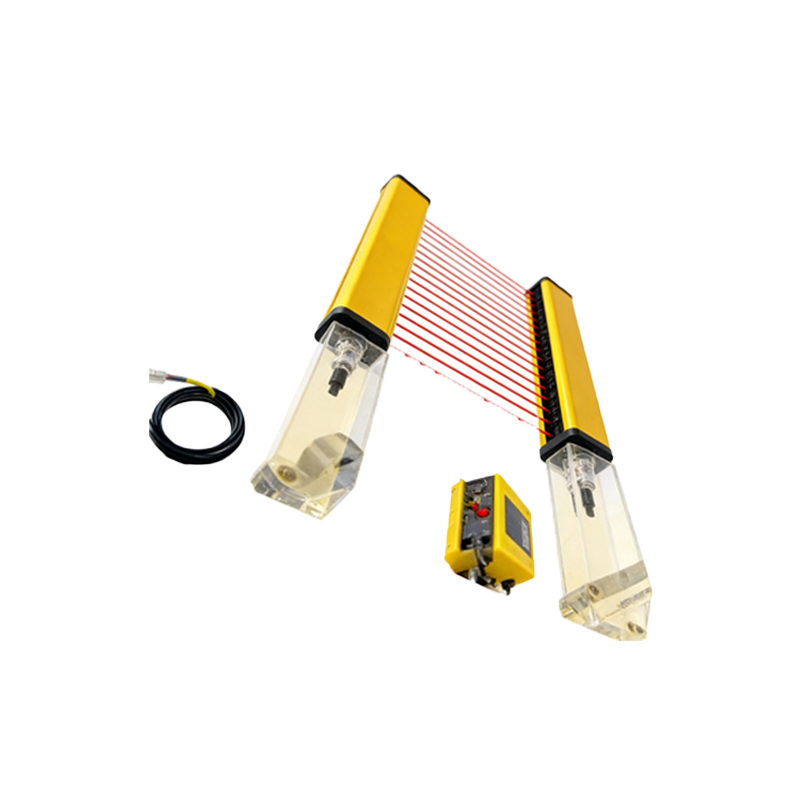
A significant portion of the schematic complexity addresses Single Event Effects. To protect against Single Event Transients (SETs) in the signal path, designers employ filtering techniques with carefully calculated RC time constants at the output of amplifier stages. This low-pass filtering helps to smooth out sharp, radiation-induced glitches before they are misinterpreted as valid signals by downstream logic. For digital control logic within smart sensors, hardening techniques are integrated into the schematic. This includes the use of Triple Modular Redundancy (TMR) for critical flip-flops and state machines, where three identical circuits vote on the correct output. While the schematic becomes threefold more complex for these blocks, it drastically reduces the probability of an SEU causing a system error. Guard rings and well ties are explicitly drawn and specified in the layout notes of the schematic to prevent latch-up, a destructive SEE.
Power Supply Conditioning and Shielding Considerations
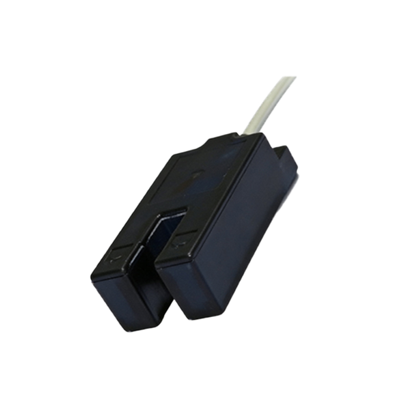
The power supply rails are a primary injection point for noise and transients caused by radiation. The schematic must include robust, rad-hard voltage regulators with current limiting and over-voltage protection. Often, local regulation is provided at each major sub-circuit to prevent fault propagation. Decoupling is aggressive, using multiple capacitors of different values (e.g., 10µF tantalum, 0.1µF ceramic) placed very close to the power pins of each integrated circuit, as indicated in the schematic notes. While physical shielding (using materials like tantalum or specialized polymers) is a mechanical design aspect, its electrical implication appears in the schematic as a dedicated grounding scheme for the shield itself. A single-point, low-impedance ground connection for the shield must be clearly defined in the schematic to avoid creating ground loops that could couple noise into the sensitive analog front-end.
Layout Guidelines Derived from the Schematic
A rad-hard schematic is inseparable from its layout requirements. The schematic document includes extensive notes and directives for the PCB designer. Key instructions include maximizing the distance between sensitive high-impedance nodes to reduce the chance of charge sharing between transistors during an ion strike. Differential signaling pairs for critical analog signals are often specified, with strict requirements for length matching and symmetry to enhance common-mode noise rejection. The use of guard traces—grounded copper pours surrounding sensitive traces—is mandated from the schematic level. Furthermore, the schematic calls for a continuous ground plane to provide a reliable return path and shielding. All these layout rules, originating from the schematic design, are crucial for realizing the radiation tolerance intended by the circuit topology.
Testing and Validation Implications
The schematic also influences the testing philosophy. Design-for-Test (DFT) features may be incorporated, such as built-in test points for injecting fault signals to simulate SEUs or measuring leakage currents that indicate TID damage. The schematic might include optional resistor placements for characterizing performance degradation over time. Validation of a rad-hard sensor involves irradiation testing (e.g., using gamma rays or heavy ions), and the schematic must be designed to facilitate this. This means including accessible measurement points for key parameters (bias voltages, amplifier outputs) without compromising the integrity of the shielding or layout. The component choices in the schematic directly determine the test protocols, as each rad-hard qualified part comes with a specific dose-rate and total dose tolerance specification.
Conclusion: The Integrated Design Philosophy
In conclusion, the schematic of a radiation-hardened photoelectric sensor is a blueprint for reliability in extreme environments. Its design is a holistic exercise combining radiation-tolerant component selection, circuit design techniques for error mitigation, and stringent layout and shielding directives. Every element, from the photodetector material to the value of a filter capacitor and the grounding of a shield, is a deliberate choice to combat the effects of ionizing radiation. It represents a convergence of physics, electrical engineering, and materials science, resulting in a device that performs a seemingly simple task—detecting light—with unwavering certainty where ordinary electronics would perish. As applications in nuclear, aerospace, and high-energy physics continue to grow, the principles embedded in these schematics will remain essential for safe and successful operations.