Introduction to Photoelectric Sensing Principles
Photoelectric sensors are fundamental components in industrial automation, utilizing light to detect the presence, absence, or distance of objects. The core principle involves an emitter, which projects a light beam (often infrared, visible red, or laser), and a receiver, which detects changes in the received light intensity. These changes are then converted into electrical signals for processing. The three primary operating modes are through-beam, retro-reflective, and diffuse reflective, each with distinct circuit implementations and considerations for ambient light immunity, sensing range, and target material. Understanding the underlying electronic circuitry is crucial for selecting the right sensor, troubleshooting system faults, and designing custom sensing solutions for complex applications. The circuit's design directly impacts critical performance parameters such as response time, switching hysteresis, and signal-to-noise ratio.
Core Components and Block Diagram
A standard photoelectric sensor circuit can be broken down into several key functional blocks. The emitter section typically consists of a light-emitting diode (LED) driven by a constant current source circuit to ensure stable light output intensity, which is vital for consistent performance over temperature variations and component aging. The receiver section houses a phototransistor or photodiode, which acts as a light-dependent current source. Following this is a signal conditioning stage, often comprising a high-gain amplifier and a filter network to amplify the weak photocurrent and reject noise, particularly from AC lighting (e.g., 50/60 Hz flicker). The conditioned signal is then fed into a comparator circuit, where it is compared against a preset threshold voltage. This threshold defines the sensor's switching point and provides adjustable sensitivity. Finally, the output stage provides a clean, digital signal (e.g., NPN/PNP transistor, relay, or solid-state switch) compatible with PLCs, counters, or other control systems. A regulated power supply unit is integral to the entire system's stability.
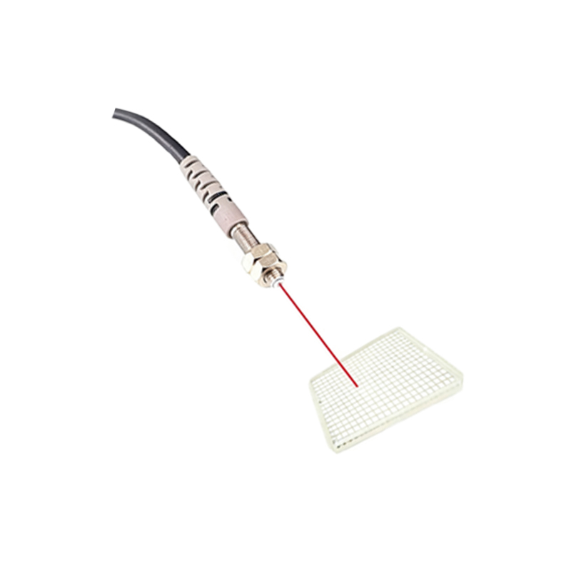
Detailed Circuit Analysis: Emitter Drive
The emitter drive circuit's primary objective is to deliver a stable, pulsed current to the LED. Pulsing the LED at a high frequency (e.g., several kHz) allows the receiver circuit to be tuned to this specific frequency, dramatically improving immunity to ambient light. A common configuration uses a 555 timer IC or a microcontroller output to generate a square wave. This signal drives the base of a transistor (BJT or MOSFET) configured as a switch. A resistor in series with the LED emitter sets the peak current. More advanced designs employ a dedicated constant-current driver IC to maintain identical light output across all production units and throughout the sensor's operational life. For long-range or laser-based sensors, the drive circuit may include feedback from a monitoring photodiode to actively regulate light intensity.
Detailed Circuit Analysis: Receiver and Signal Conditioning
The phototransistor is typically connected in a common-emitter configuration. When light strikes its base, it allows collector current to flow, producing a voltage drop across a load resistor. This small analog voltage is highly susceptible to noise. The first amplification stage often uses a low-noise operational amplifier (op-amp) in a transimpedance configuration for photodiodes or a non-inverting amplifier setup for phototransistors. Following amplification, a band-pass filter is critical. It is centered on the emitter's modulation frequency, rejecting low-frequency ambient light drift and high-frequency electrical noise. The quality factor (Q) of this filter determines the selectivity and thus the sensor's ability to distinguish its own signal from background interference. Proper PCB layout, with guarding and short traces, is essential in this high-gain stage to prevent oscillation and capacitive pickup.
The Comparator and Hysteresis
The clean, amplified AC signal is rectified and smoothed to produce a DC voltage proportional to the received light intensity. This DC voltage is fed to the inverting input of a comparator op-amp. A potentiometer or digital-to-analog converter (DAC) sets a reference voltage on the non-inverting input, which serves as the sensitivity adjustment. A crucial feature here is the addition of positive feedback to create hysteresis. This introduces two distinct thresholds: one for turning the output ON and a lower one for turning it OFF. Hysteresis prevents output chatter or oscillation when the sensed signal is near the switching point, such as with a dirty or vibrating object. The value of the hysteresis resistor network is calculated based on the desired difference between the ON and OFF light levels.
Output Stage and Protection Circuits
The comparator's output drives the final output stage. For a standard NPN (sinking) or PNP (sourcing) transistor output, a BJT or MOSFET is used to switch the load connected to the supply voltage. Protection components are paramount. A flyback diode is placed across inductive loads (like relays) to suppress voltage spikes. Current-limiting resistors protect the output transistor from short circuits. For sensors in harsh electrical environments, additional protection against surge voltages, electromagnetic interference (EMI), and reverse polarity is implemented using transient voltage suppression (TVS) diodes, ferrite beads, and series diodes. Opto-isolators are sometimes used to electrically separate the sensitive signal conditioning circuitry from the noisy output switching stage, enhancing reliability.
Design Considerations and Best Practices
When designing or applying photoelectric sensor circuits, several factors must be optimized. Lens selection for both emitter and receiver affects the beam shape and sensing range. The modulation frequency must be chosen to avoid interference from other light sources and to allow for a fast enough response time. Power supply decoupling with capacitors near each IC is non-negotiable for stable operation. Environmental factors like temperature will affect LED output and phototransistor gain; temperature compensation circuits may be necessary for precision applications. For diffuse sensors, background suppression designs use triangulation with dual receiver elements or specialized PSD (Position Sensitive Device) circuits to ignore objects beyond a set distance. Always consult manufacturer datasheets for absolute maximum ratings and application notes.
Troubleshooting Common Circuit Issues
Common failures can be diagnosed by analyzing the circuit stage by stage. No output may indicate a failed emitter LED, which can be checked with an infrared viewer or by measuring current draw. Erratic operation often points to insufficient hysteresis, noise ingress due to poor shielding, or an incorrectly set sensitivity threshold. Reduced sensing range can be caused by a degraded emitter (diminished light output), dirty lenses, or a faulty component in the amplifier stage lowering the gain. Using an oscilloscope to probe the signal at the amplifier output and comparator input is the most effective method to visualize noise levels, signal strength, and the switching behavior. Always verify the power supply voltage and check for cold solder joints or damaged PCB traces.