Introduction to 520nm Photoelectric Sensors
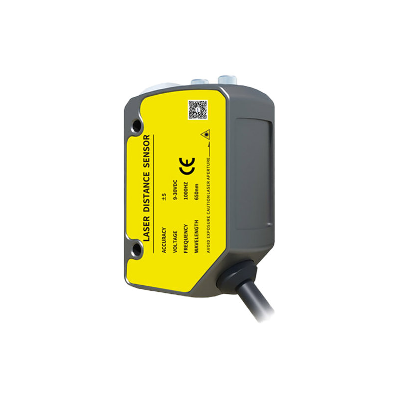
A 520nm photoelectric sensor is a specialized optoelectronic device designed to detect, measure, or respond to light at a wavelength of 520 nanometers, which corresponds to a vibrant green hue in the visible spectrum. The image of such a sensor typically reveals a compact, robust housing, often constructed from industrial-grade plastics or metals, featuring a clearly marked emitter and receiver window. Internally, the core components include a light-emitting diode (LED) that precisely emits light at 520nm and a phototransistor or photodiode receiver. The visual representation is crucial for engineers, as it allows for the identification of key physical features such as the sensing face alignment, mounting brackets, connection ports, and status indicator LEDs. High-quality images often highlight the sensor's form factor, ingress protection (IP) rating seals, and lens type, providing immediate visual cues about its suitability for specific environmental conditions, such as resistance to dust, moisture, or chemical exposure.
Interpreting Key Features from Sensor Imagery
Analyzing a 520nm photoelectric sensor image goes beyond aesthetics; it is a functional assessment. The first element to examine is the optical path configuration. Images clearly show whether the sensor is of a through-beam, retro-reflective, or diffuse-reflective type. The housing design and window placement offer direct visual evidence. For instance, a through-beam sensor image will show two separate units—an emitter and a receiver—with distinct, aligned apertures. A close-up image of the sensing face reveals the lens quality and any built-in filters, which are critical for minimizing interference from ambient light, a common challenge with 520nm light in environments with strong green or white background illumination. Furthermore, labels for connection types (e.g., M8 or M12 connectors) and wiring diagrams, if visible in the image, are essential for planning system integration.
The Significance of 520nm Wavelength Selection
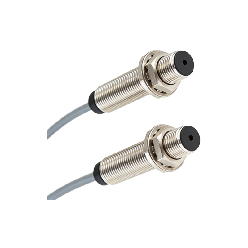
The choice of 520nm green light is a deliberate engineering decision, clearly justified when considering the sensor's application context. This specific wavelength offers a distinct advantage in contrast detection. In industrial settings, many objects—brown cardboard, blue plastic components, metallic surfaces—reflect or absorb green light differently than red or blue light. Therefore, a sensor image emphasizing its 520nm capability signals its optimization for high-contrast detection on colored objects or against colored backgrounds. It is less susceptible to interference from certain types of ambient artificial light, like standard red LEDs. The monochromatic nature of the emitted light, as suggested by the specification, implies a focused sensitivity, reducing false triggers and enhancing signal stability compared to broad-spectrum sensors.
Common Industrial Applications and Use-Cases
The practical deployment of 520nm photoelectric sensors is vast. High-resolution images often depict these sensors in action within automated systems. A prevalent application is in packaging and labeling machinery, where the sensor verifies the presence or position of labels, particularly those with specific color codes or registration marks. The green light provides excellent contrast against white or silver label backings. Another critical use is in electronic assembly lines for detecting components on tape-and-reel feeders or verifying solder paste application. Images from automotive manufacturing show these sensors ensuring the correct placement of colored wiring harnesses or fluid levels in translucent reservoirs, where the 520nm light offers a clear reflective or transmissive signal. In printing, they monitor paper jams or color registration by detecting marks printed with inks that absorb green light.
Technical Considerations for Optimal Performance
To achieve the performance implied by a sensor's image and specifications, several technical parameters must be aligned. The sensing range, indicated by specifications but often inferred from the lens design in images, must match the application distance. The response time, a critical factor in high-speed automation, is not visible in a static image but is a key specification linked to the internal circuitry hinted at by the sensor's size and component density. Environmental robustness, visually suggested by IP-rated seals and sturdy housing in product images, is paramount. For a 520nm sensor, ensuring a clean lens free of obstructions is vital, as dirt or condensation can scatter or absorb the specific wavelength, drastically reducing sensitivity. Proper alignment, as guided by the housing geometry visible in images, is also essential for reliable operation.
Integration and Installation Best Practices
A well-composed product image serves as an initial installation guide. It shows the recommended mounting points, often via integrated brackets or threaded barrels. The orientation of the emitter and receiver, if separate units, is clearly depicted. For integration, the wiring connection type is visually apparent. Best practices derived from such imagery include ensuring a stable, vibration-free mount to maintain optical alignment, avoiding mounting surfaces that could cause reflective interference (a potential issue with shiny surfaces and 520nm light), and providing adequate clearance for cable bending as shown at the sensor's connector exit point. Installing the sensor at a slight angle, as sometimes demonstrated in application diagrams, can help avoid direct specular reflection from glossy target surfaces back into the receiver.
Advancements and Future Trends in Sensor Imaging
Modern product imaging for components like 520nm photoelectric sensors is evolving beyond simple photographs. Manufacturers now provide detailed 2D and 3D CAD model images for direct integration into machine design software. These technical images allow for precise spatial planning before physical installation. Furthermore, the sensors themselves are advancing. Future iterations may incorporate smart features like IO-Link connectivity, which would be indicated in product images by additional communication ports or status LEDs. There is also a trend toward miniaturization and enhanced environmental sealing, visible in the increasingly compact and seamless housing designs shown in latest product images. The core principle of using 520nm light for superior contrast detection remains, but the packaging and intelligence surrounding it continue to progress, as vividly captured in contemporary technical imagery.