Introduction to Photoelectric Proximity Sensing
Photoelectric proximity sensors are indispensable components in modern industrial automation, offering non-contact detection of objects. Unlike inductive or capacitive sensors, they utilize light beams to sense presence, distance, or absence, making them versatile for diverse materials including glass, plastic, and metal. The core principle revolves around the emission, reflection, or interruption of a light signal, which is then converted into an electrical output. Understanding the schematic diagram of such a sensor is crucial for engineers involved in system design, troubleshooting, and integration. This article delves into the typical schematic, breaking down each functional block to elucidate how these reliable devices operate from an electrical and optical standpoint.
Core Components and Functional Blocks
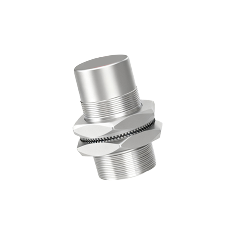
A standard photoelectric proximity sensor schematic can be divided into several key sections. The primary blocks include the Light Emitter (usually an LED or Laser Diode), the Light Receiver (a phototransistor, photodiode, or photoelectric cell), the Signal Processing Circuit, and the Output Stage. The emitter circuit is driven by a constant current source to ensure stable light intensity, often modulated at a specific frequency to mitigate ambient light interference. The receiver circuit is designed to be highly sensitive to this specific modulated frequency while filtering out DC light and noise. The signal processing block typically involves amplification, demodulation, and comparison stages to transform the tiny photocurrent from the receiver into a clean, decisive logic signal.
The Emitter Circuit Schematic Detail
Focusing on the emitter side, the schematic shows the light-emitting diode (LED) connected in series with a current-limiting resistor and a transistor switch. The LED is often pulsed by an oscillator circuit running at frequencies between 1kHz to 50kHz. This modulation is critical. The schematic details how the oscillator, which could be a simple 555 timer IC or part of the sensor's dedicated ASIC, controls the transistor's base, switching the LED on and off rapidly. A constant-current driver circuit might be incorporated to maintain consistent luminous output regardless of minor voltage fluctuations or temperature changes, ensuring long-term stability and detection repeatability.
The Receiver and Amplification Stage
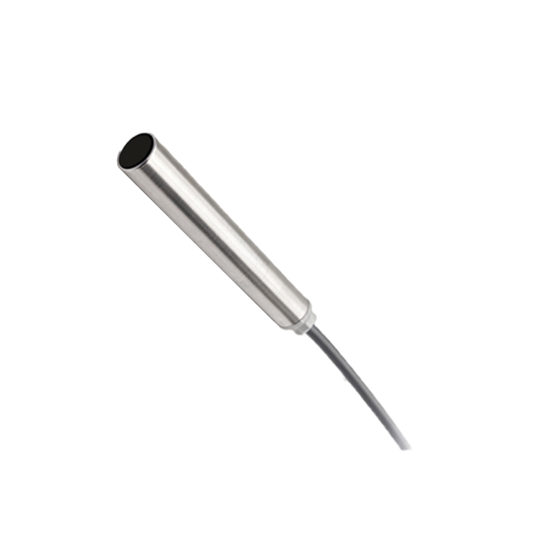
On the receiver end, the photodetector, such as a phototransistor, is biased in its active region. When the modulated light from the emitter strikes its base region, it generates a collector current proportional to the light intensity. This minute current is fed into a high-gain operational amplifier configured as a transimpedance amplifier. This stage converts the current signal into a usable voltage. The schematic clearly depicts the feedback resistor and capacitor in this op-amp circuit, which set the gain and bandwidth, effectively amplifying the weak signal while minimizing noise pickup.
Demodulation and Signal Conditioning
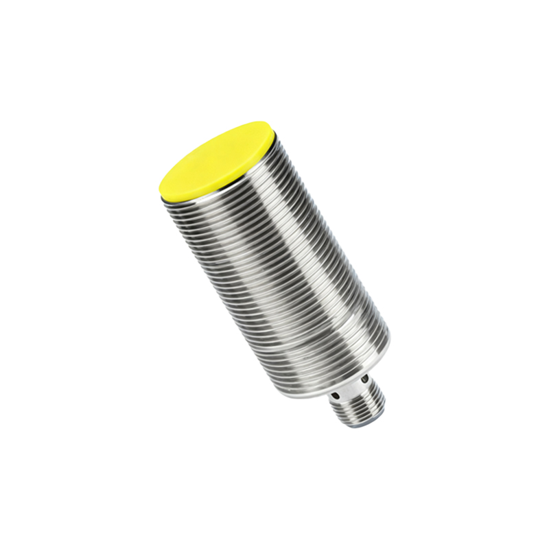
Following amplification, the signal enters the demodulation stage. Since the received signal contains the modulated carrier frequency from the emitter, it must be extracted. The schematic illustrates a synchronous demodulator or a simple envelope detector circuit that strips away the carrier, leaving behind a DC voltage level that corresponds to the presence or strength of the received light. This DC signal is then passed through a low-pass filter to smooth it out before being sent to a comparator. The comparator circuit compares this conditioned voltage against a preset threshold voltage, set by a potentiometer or fixed resistors, to determine the object's presence.
Output Stage and Switching Logic
The output of the comparator drives the final output stage. Common output configurations shown in schematics include NPN/PNP transistors for DC sensors or electromechanical relays for AC/DC models. For a standard NPN sinking output, the schematic shows an NPN transistor whose collector is connected to the load and emitter to ground. When the comparator's output goes high (object detected or not detected, depending on light-on/dark-on mode), it saturates this output transistor, allowing current to flow from the load to ground, thus switching the external circuit. Protection components like flyback diodes for inductive loads or snubber circuits are often included in this section of the schematic.
Power Supply and Regulation
A robust power supply section is vital. The schematic includes a voltage regulator IC (like a 78xx series) or a more sophisticated switching regulator to provide stable DC voltage (e.g., 5V or 12V) from a wider input range (10-30V DC) to all internal circuits. Decoupling capacitors are placed near each IC's power pins to filter high-frequency noise. This section ensures that the sensitive analog amplification and comparison circuits operate without being affected by power line disturbances, which is paramount for reliable operation in electrically noisy industrial environments.
Schematic Variations for Sensing Modes
The fundamental schematic varies based on the sensing