Introduction to Hall Effect Proximity Sensor Manufacturing
The production of Hall Effect proximity sensors represents a sophisticated intersection of semiconductor technology, precision engineering, and robust quality control. As a cornerstone of modern industrial automation, these non-contact sensors detect the presence of ferromagnetic objects by sensing changes in a magnetic field. Leading manufacturers operate within highly controlled environments, utilizing advanced processes to ensure the reliability, accuracy, and longevity required for demanding applications in automotive, aerospace, robotics, and factory automation. The journey from raw silicon to a fully packaged, tested sensor involves numerous critical stages, each demanding meticulous attention to detail.
Core Semiconductor Fabrication and Die Production
The heart of any Hall Effect sensor is its semiconductor die. Production begins in specialized cleanroom facilities where high-purity silicon wafers undergo a series of photolithographic, etching, and doping processes. These steps define the microscopic Hall plate—the sensitive element that generates a voltage proportional to the applied magnetic field. Precision is paramount; even nanometer-scale variations can affect sensitivity and offset voltage. After fabrication, the wafers are subjected to rigorous electrical testing at the wafer level. Automated probe stations map the performance of each individual die, identifying and marking those that meet stringent electrical specifications for sensitivity, linearity, and temperature stability before the wafer is diced.
Advanced Assembly and Packaging Techniques
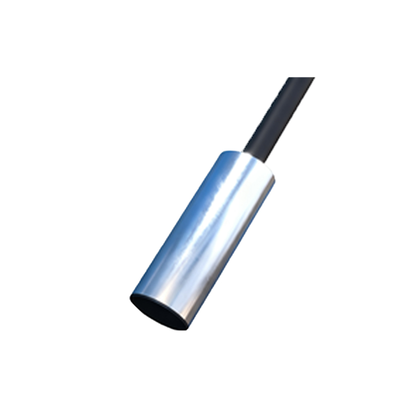
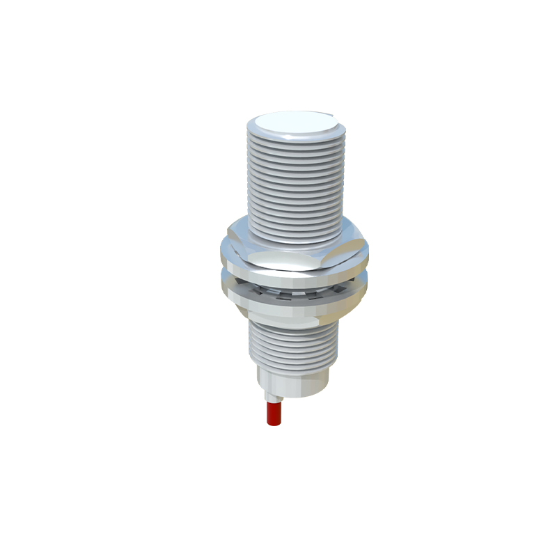
Once singulated, the qualified dies are transferred to assembly lines. Here, they are precisely placed and bonded onto lead frames or substrate packages using automated die-attach systems. The critical electrical connections from the die to the package leads are established via ultra-fine gold or aluminum wire bonding. This stage requires exceptional precision to ensure signal integrity and mechanical strength. The assembly is then encapsulated in a protective molding compound, typically a thermoset epoxy resin. This encapsulation safeguards the delicate semiconductor structure from environmental hazards such as moisture, dust, chemicals, and mechanical stress. For specialized applications, manufacturers may employ custom packages with integrated magnets or shielding to optimize magnetic field interaction.
Calibration, Programming, and Final Testing
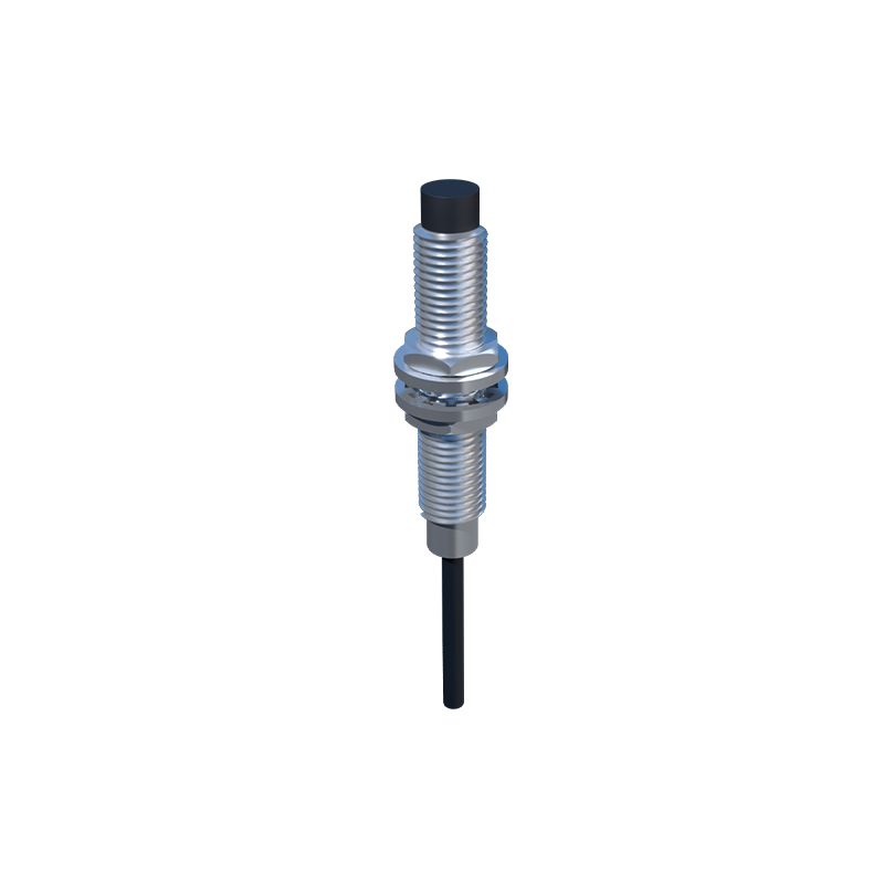
Post-encapsulation, the sensors enter the calibration and programming phase. This is where generic components are transformed into application-specific devices. Using automated test equipment (ATE), each sensor is exposed to precisely controlled magnetic fields across its operational temperature range. Calibration parameters, such as quiescent output voltage, sensitivity (mV/G), and switch points, are measured and adjusted. For programmable digital sensors (e.g., I2C or PWM output), specific thresholds and output formats are written to on-chip memory. Final testing is exhaustive, verifying all key parameters: magnetic switch points, hysteresis, response time, supply current, output current capability, and protection against reverse polarity and overvoltage. Only units passing 100% of these tests proceed.
Stringent Quality Assurance and Reliability Protocols
A hallmark of a premier Hall Effect proximity sensor manufacturer is an unwavering commitment to quality. This extends beyond final testing to encompass the entire production lifecycle. Statistical Process Control (SPC) monitors every critical production parameter in real-time. Reliability testing, conducted on sample batches, simulates years of operation through accelerated life tests, including high-temperature operating life (HTOL), temperature cycling, humidity exposure, and mechanical shock/vibration tests. Compliance with international standards like ISO 9001, IATF 16949 for automotive, and AEC-Q100 is mandatory for suppliers to major industries. This rigorous approach minimizes infant mortality failures and ensures consistent performance in the field.
Innovation and Future Trends in Sensor Production
The manufacturing landscape is continuously evolving. Leading factories are integrating Industry 4.0 principles, utilizing IoT-enabled machinery for predictive maintenance and data analytics to further optimize yield and quality. There is a strong trend towards miniaturization, producing sensors in ultra-small packages like DFN or wafer-level chip-scale packages (WLCSP) for portable electronics. Furthermore, the integration of additional functionalities—such as signal conditioning, diagnostics, and bus interfaces—onto a single chip (creating "smart sensors") is becoming standard. Research into new materials, like graphene or advanced III-V compounds, promises future sensors with higher sensitivity, wider temperature ranges, and lower power consumption, driving the next generation of manufacturing innovation.