Introduction to Photoelectric Sensor Transistors
A photoelectric sensor transistor is a fundamental semiconductor component that combines the light-sensing capability of a photodiode with the signal amplification function of a bipolar junction transistor (BJT). At its core, it is a transistor whose base current is controlled by incident light rather than an electrical signal. When light photons of sufficient energy strike the base-collector junction, they generate electron-hole pairs, creating a photocurrent that acts as the base current. This photocurrent is then amplified by the transistor's gain, resulting in a significantly larger collector current that can be easily measured or used to drive other circuits. This intrinsic amplification makes phototransistors far more sensitive to light than simple photodiodes, making them ideal for a wide range of detection and switching applications in industrial automation, consumer electronics, and safety systems.
Core Operating Principles and Structure
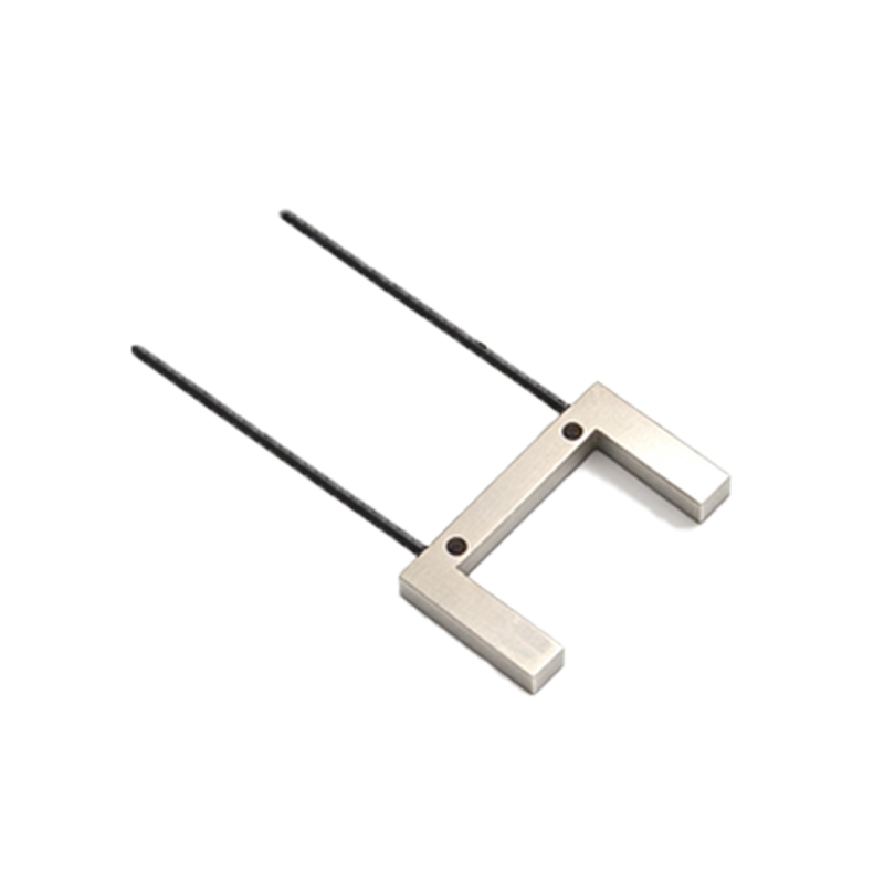
The typical structure of a phototransistor resembles a standard NPN or PNP bipolar transistor, but with a crucial modification: the package includes a lens to focus light onto the semiconductor die, and the base terminal is often left unconnected or is used for bias adjustment. In the most common NPN configuration, with the collector at a positive voltage relative to the emitter, the base-collector junction is reverse-biased. In darkness, only a tiny leakage current (dark current) flows. When light illuminates the base region, photons generate charge carriers. These carriers are swept across the junction by the electric field, initiating a base current. The transistor's current gain (hFE or β) multiplies this current, so the final collector current (I_C) is approximately β times the photogenerated base current. This is why even low light levels can produce a usable output signal. Key parameters include spectral response (peak sensitivity wavelength, often in the near-infrared or visible range), collector-emitter breakdown voltage, rise/fall time (response speed), and collector dark current.
Key Types and Variations
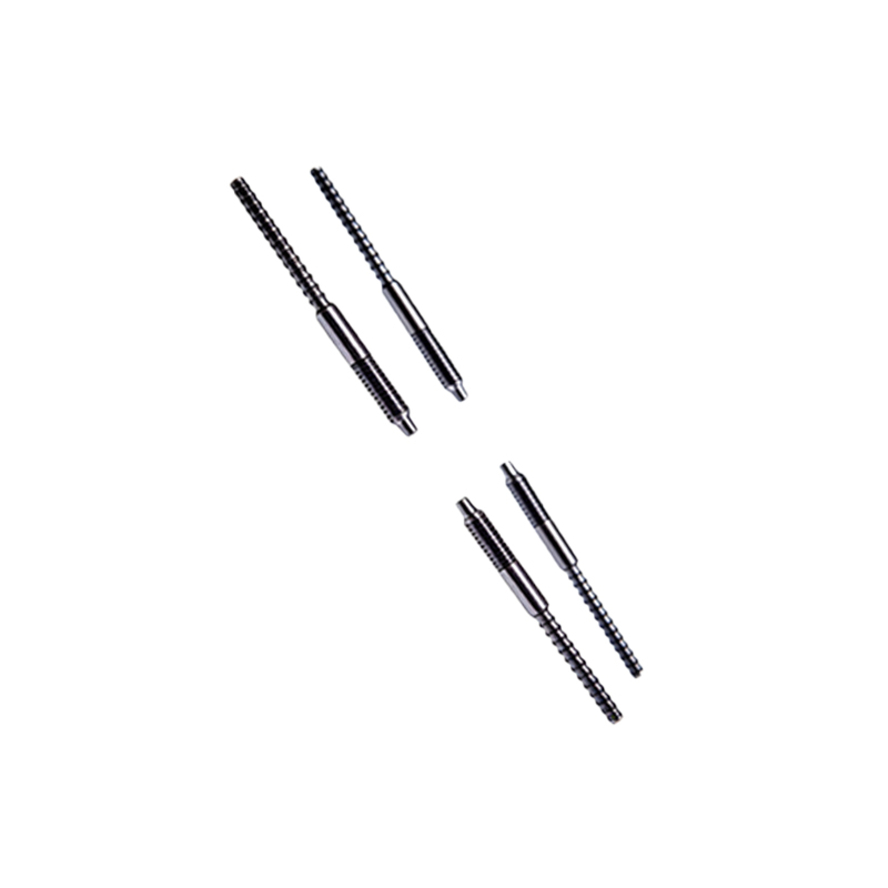
Several specialized types of phototransistors have been developed to meet specific application needs. The standard phototransistor is a two-lead device (collector and emitter). A photodarlington transistor incorporates a second transistor stage to provide extremely high gain, suitable for detecting very faint light, though at the cost of slower response times and higher saturation voltage. For applications requiring precise signal control or compensation for temperature variations, a phototransistor with an accessible base lead is used, allowing external biasing. Silicon is the most common material, offering a good response to visible and near-infrared light. For specific wavelength bands, materials like germanium or gallium arsenide are employed. Furthermore, many modern devices are integrated into optocouplers or optoisolators, where an infrared LED is paired with a phototransistor in a single, light-tight package to provide electrical isolation between circuits, a critical feature for safety and noise immunity.
Primary Industrial and Commercial Applications
The high sensitivity and solid-state reliability of phototransistors make them ubiquitous in automation and sensing. In industrial settings, they are the core component in object detection sensors, counting items on conveyor belts, detecting the presence or absence of parts in assembly machines, and reading encoder disks for position and speed feedback. Consumer electronics utilize them in devices like TV remote control receivers, ambient light sensors for automatic display brightness adjustment, and paper detection in printers. Safety systems rely on phototransistors in smoke detectors, where scattered light from smoke particles triggers an alarm, and in safety curtains or light barriers that halt machinery when a beam is interrupted. Their use in optoisolators is critical in motor drives, power supplies, and medical equipment to separate high-voltage circuits from low-voltage control logic, preventing dangerous fault propagation and ground loops.
Critical Selection Criteria for Engineers
Selecting the right phototransistor requires careful consideration of multiple parameters. First, match the spectral response to the light source; an infrared phototransistor must be paired with an IR LED. Sensitivity or collector current for a given light intensity (often measured in mW/cm²) determines the detection range and needed amplification. Response speed, defined by rise and fall times, is paramount for high-speed counting or data communication; standard devices may be too slow for pulsed applications. The collector-emitter voltage rating must exceed the circuit's supply voltage. Package style is also crucial: epoxy-coated devices are cost-effective, while hermetically sealed metal-can packages offer better performance in harsh environments. For designs sensitive to noise or temperature drift, choosing a device with a base lead for external compensation circuits can be advantageous. Always consult the manufacturer's datasheet for graphs showing output current versus light intensity and response time versus load resistance.
Advantages, Limitations, and Comparison with Alternatives
The primary advantage of the phototransistor is its high gain, providing a strong output signal without additional amplification stages, which simplifies circuit design and reduces cost. They are generally robust, long-lasting, and immune to contact bounce issues found in mechanical switches. However, they have distinct limitations. Their response time is slower than that of a photodiode, making photodiodes preferable for very high-frequency or precision analog light measurement applications. Phototransistors are also more sensitive to temperature variations, which can affect the dark current and gain. Saturation effects can limit their use in linear analog circuits. Compared to a photodiode-transistor combination in a separate configuration, the integrated phototransistor is simpler but offers less design flexibility. For the highest sensitivity to low light, an avalanche photodiode (APD) or a photomultiplier tube is used, though these are significantly more complex and expensive.
Practical Circuit Design Considerations
A typical switching circuit uses a phototransistor in a common-emitter configuration. The collector is connected to the positive supply via a pull-up resistor (R_L), and the emitter is grounded. The output voltage is taken from the collector node. In darkness, the phototransistor is off, and the output is high (near Vcc). When light strikes the transistor, it turns on, pulling the output voltage low. The value of R_L is a critical design choice: a larger resistor increases sensitivity (a larger voltage swing for a given light current) but slows down the response time due to increased RC time constant with the transistor's capacitance. For analog light measurement, a transimpedance amplifier circuit using an operational amplifier can convert the phototransistor's output current into a precise voltage, though careful design is needed to ensure stability and bandwidth. Proper shielding from unwanted ambient light and electrical noise is essential for reliable operation, often achieved by using modulated light sources and synchronous detection in demanding environments.