Introduction to Photoelectric Sensors
Photoelectric sensors are essential components in modern automation and control systems, converting light signals into electrical outputs. These devices rely on precise structural assembly to ensure reliable performance in diverse industrial environments. The assembly process involves integrating optical, electronic, and mechanical parts with high accuracy. This guide outlines key steps and considerations for assembling photoelectric sensors, adhering to industry standards for durability and functionality. Proper assembly not only enhances sensor efficiency but also extends its operational lifespan in applications like object detection, positioning, and safety systems.
Key Components and Materials
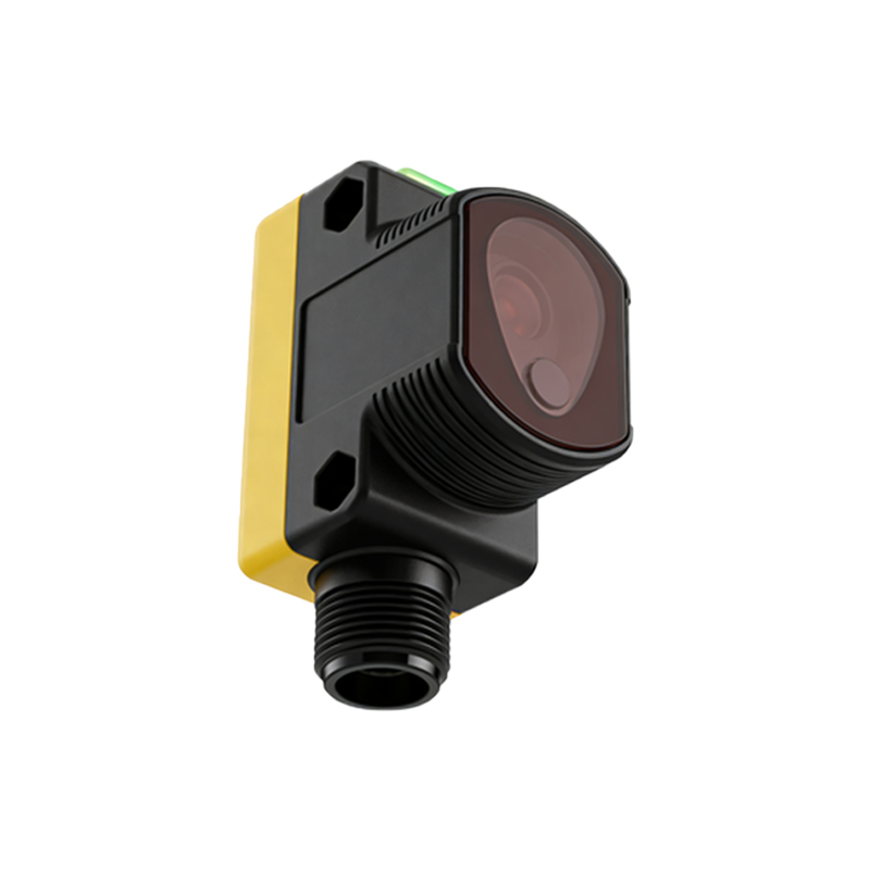
The core components of a photoelectric sensor include an emitter (light source), receiver (photodetector), housing, lens, and electronic circuitry. Emitters typically use LEDs or laser diodes, while receivers consist of phototransistors or photodiodes. The housing, often made from durable plastics or metals like aluminum, provides protection against environmental factors such as dust, moisture, and mechanical shocks. Lenses, crafted from materials like polycarbonate or glass, focus light beams to improve sensing range and accuracy. Electronic circuits, including amplifiers and signal processors, are mounted on PCBs within the housing. Selecting high-quality materials ensures resistance to temperature fluctuations and chemical exposure.
Assembly Process Overview
Assembly begins with preparing the housing by cleaning and inspecting for defects. The emitter and receiver are then precisely aligned on the PCB, using automated tools to maintain optical axis consistency. Soldering connects these components to the circuit, followed by securing the PCB inside the housing with screws or adhesives. Lenses are installed over the optical elements, often with sealing gaskets to prevent contamination. Wiring for power and output signals is routed through cable glands, ensuring strain relief. Finally, the housing is sealed, typically with ultrasonic welding or epoxy, to achieve an IP rating for ingress protection. Each step requires strict adherence to torque specifications and alignment tolerances.
Alignment and Calibration Techniques
Accurate alignment between the emitter and receiver is critical for optimal sensor performance. This involves using jigs and fixtures to position components within micron-level tolerances. Calibration is performed by testing the sensor's response to standardized light intensities, adjusting circuit potentiometers or software parameters as needed. Automated calibration systems measure output signals under varying conditions, such as different distances or ambient light levels, to ensure consistent detection. Regular checks during assembly prevent misalignment caused by thermal expansion or vibration. Proper calibration guarantees that the sensor meets specified sensing ranges and response times, reducing false triggers in real-world applications.
Quality Control and Testing
Quality control in photoelectric sensor assembly includes visual inspections, electrical tests, and environmental simulations. Inspectors verify component placement, solder joints, and housing integrity. Electrical tests assess output signals, response latency, and power consumption using oscilloscopes and multimeters. Environmental testing subjects sensors to conditions like high humidity, extreme temperatures, and vibration to validate durability standards such as IEC 60947-5-2. Additionally, functional tests involve passing objects through the sensing field to check detection reliability. Data from these tests are logged for traceability, ensuring each sensor meets industry certifications before shipment.
Common Challenges and Solutions
During assembly, challenges include component misalignment, signal interference, and sealing failures. Misalignment can be mitigated by using precision alignment tools and regular calibration checks. Signal interference from ambient light or electrical noise is addressed by incorporating shielding in the housing and filtering circuits. Sealing issues, which compromise IP ratings, are resolved by selecting appropriate gasket materials and verifying seal integrity with pressure tests. Training assemblers on best practices and implementing automated inspection systems also reduce human error. By proactively addressing these issues, manufacturers enhance sensor reliability and reduce warranty claims.
Applications and Industry Trends
Assembled photoelectric sensors are widely used in manufacturing, packaging, automotive, and robotics industries. They enable tasks like counting products on conveyor belts, detecting object presence in machinery, and ensuring safety in automated systems. Current trends focus on miniaturization, with sensors becoming smaller yet more powerful through advanced micro-optics and integrated circuits. Smart sensors with IoT connectivity are gaining popularity, allowing real-time monitoring and diagnostics. Additionally, eco-friendly materials and energy-efficient designs are emerging to support sustainability goals. As automation evolves, precise assembly remains vital for next-generation sensors with enhanced sensitivity and connectivity features.
Conclusion and Best Practices
Successful photoelectric sensor assembly hinges on meticulous attention to detail, from component selection to final testing. Best practices include maintaining a clean assembly environment to avoid contamination, using calibrated tools for alignment, and adhering to standardized protocols for sealing and wiring. Regular training for technical staff ensures up-to-date knowledge of assembly techniques and quality standards. By following these guidelines, manufacturers can produce robust sensors that deliver consistent performance in demanding industrial settings. Continuous improvement in assembly processes will drive innovation, supporting the growing demand for reliable automation solutions worldwide.