The Rise of Miniaturization in Sensing Technology
The industrial automation landscape is undergoing a profound transformation, driven by the relentless demand for higher efficiency, greater precision, and space optimization. At the heart of this evolution lies the photoelectric sensor, a workhorse for object detection, positioning, and quality control. In recent years, the focus has sharply turned towards ultra-compact photoelectric sensor manufacturers who are pioneering a new era of miniaturization. These innovators are not merely shrinking existing designs; they are re-engineering core components and packaging to deliver full-featured sensing performance in footprints previously unimaginable. This shift enables machine builders and system integrators to design sleeker, more complex, and densely packed equipment without compromising on detection capabilities. The push for smaller sensors is intrinsically linked to trends like collaborative robotics, compact machinery, and the need for more sensors per unit area in high-speed production lines.
Key Innovations from Leading Manufacturers
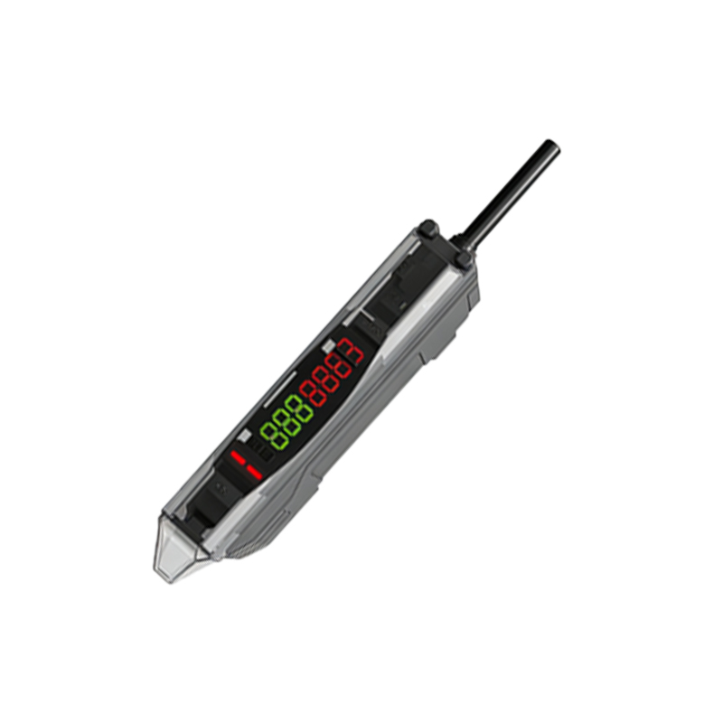
Leading ultra-compact photoelectric sensor manufacturers distinguish themselves through several critical technological advancements. Firstly, breakthroughs in LED and laser diode technology allow for powerful, focused beams from tiny emitters, ensuring long sensing ranges and high energy efficiency even in miniature housings. Secondly, advanced ASIC (Application-Specific Integrated Circuit) design integrates signal processing, amplification, and communication protocols onto a single chip, drastically reducing the internal PCB size and power consumption. Thirdly, sophisticated optical design, including precision-molded lenses and light guides, maximizes light collection and rejection of ambient interference. Manufacturers like Omron, Sick, Keyence, Banner Engineering, and Panasonic are at the forefront, offering sensors with housings as small as a few cubic centimeters. These units often feature built-in amplifiers, multiple output types (NPN/PNP, analog, IO-Link), and advanced functions like background suppression or precise color recognition, all packed into a rugged, IP67-rated enclosure.
Critical Selection Criteria for System Designers
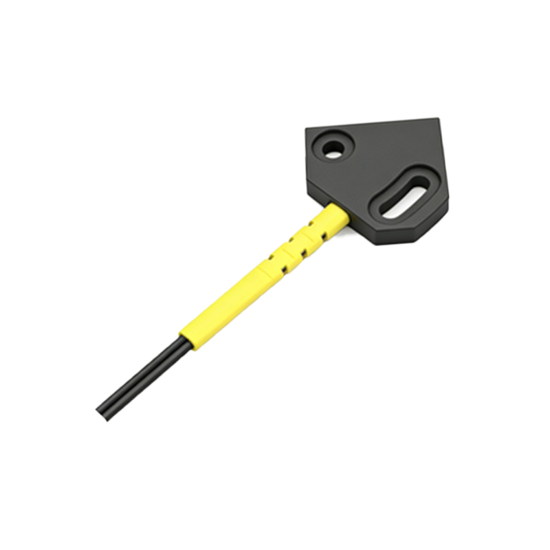
Choosing the right ultra-compact photoelectric sensor requires careful consideration beyond mere size. Key performance parameters include sensing range, which must be adequate for the application despite the small form factor. Beam type is another crucial factor; diffuse, retro-reflective, and through-beam models are available in miniature versions, each with trade-offs in range, setup simplicity, and environmental robustness. Response time is paramount for high-speed applications, with top-tier miniature sensors achieving sub-millisecond switching. The choice of light source—red visible, infrared, or laser—impacts precision, visibility for alignment, and resistance to ambient light. Furthermore, connectivity is evolving; support for smart sensor protocols like IO-Link is becoming a standard expectation, enabling parameter setting, condition monitoring, and seamless integration into Industry 4.0 data ecosystems from these tiny devices.
Dominant Applications Driving Market Demand
The adoption of ultra-compact photoelectric sensors is exploding across diverse sectors. In electronics manufacturing, they are indispensable for verifying micro-component placement on PCBs, detecting tiny leads, and ensuring proper alignment in pick-and-place robots. The pharmaceutical and packaging industries utilize them for precise tablet counting, label verification on small vials, and detecting minuscule defects in blister packs. Collaborative robot (cobot) arms rely on these sensors for safe, close-proximity end-of-arm tooling and part presence detection without adding bulky payloads. Mobile robots and AGVs use them for compact bumper and cliff detection systems. Additionally, they are vital in semiconductor fabrication, medical device assembly, and anywhere stringent hygiene standards require sensors that leave minimal surface area for contamination.
Overcoming Challenges with Advanced Engineering
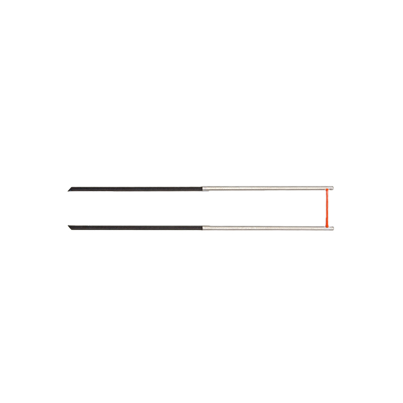
Designing reliable ultra-compact photoelectric sensors presents significant challenges that manufacturers continuously overcome. Thermal management is critical, as dense electronics in a small space can generate heat that affects LED lifespan and circuit stability. Advanced materials and efficient circuit design are employed to dissipate heat effectively. Resistance to environmental factors like washdown chemicals, oils, and mechanical vibration must be maintained, leading to innovations in potting compounds and housing seals. Ensuring easy installation and alignment is another hurdle, addressed with intuitive mounting brackets, built-in alignment indicators (like visible red beams or precise spot lasers), and simple push-button teach functions. The goal is to deliver a sensor that is not only small and powerful but also exceptionally user-friendly and durable in harsh industrial settings.
The Future: Smarter, More Integrated, and Connected
The trajectory for ultra-compact photoelectric sensor manufacturers points toward even greater intelligence and integration. The convergence of sensing and processing will deepen, with more onboard diagnostics and self-adaptive capabilities. We will see wider adoption of multi-pixel technology in tiny formats, allowing for precise edge detection and profile measurement. Wireless connectivity options may become more prevalent for hard-to-reach installations. Furthermore, the synergy with AI and machine learning at the network edge will enable these small sensors to make preliminary decisions, filtering data before sending it to higher-level controllers. As the Industrial Internet of Things (IIoT) matures, the ultra-compact photoelectric sensor will evolve from a simple detection switch into a critical, intelligent node in a vast, data-driven production network, all while occupying a minuscule physical footprint.