Introduction to Photoelectric Sensing Principles
Photoelectric sensors operate on the fundamental principle of converting light signals into electrical signals. The core function involves a light emitter, typically an LED or laser diode, and a light receiver, such as a phototransistor, photodiode, or in some advanced cases, a CMOS or CCD array. The internal circuitry is designed to precisely control the emission of light and to sensitively detect its presence, absence, or modulation after interacting with a target object. Variations in the received light intensity are translated into clean, usable electrical output signals, which form the basis for detection, counting, positioning, and other automation tasks. Understanding the schematic that governs this process is crucial for selecting the right sensor, troubleshooting failures, and designing effective integration into larger control systems.
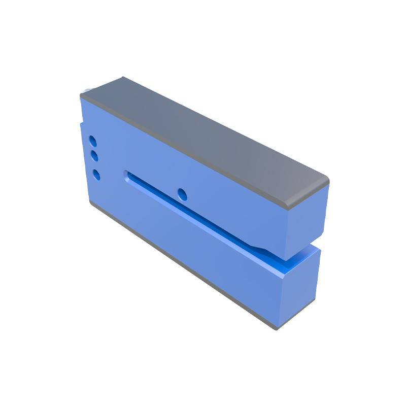
Core Components and Their Schematic Representation
A typical photoelectric sensor circuit can be broken down into several key blocks, each with a distinct schematic representation. The Emitter Circuit centers around the light-emitting element (D1). It is driven by a constant current source or a pulsed driver circuit to ensure stable light output intensity and longevity. This circuit often includes a series current-limiting resistor and may incorporate feedback from a monitoring photodiode within the LED package for closed-loop intensity control. The Receiver Circuit begins with the photodetector (Q1 or PD1). For a phototransistor, the schematic shows the device with its collector and emitter, often with a pull-up resistor at the collector to define the output voltage swing. Photodiodes are typically shown in reverse-bias configuration, connected to a transimpedance amplifier (TIA) to convert the minute photocurrent into a measurable voltage.
Signal Conditioning and Amplification Stage
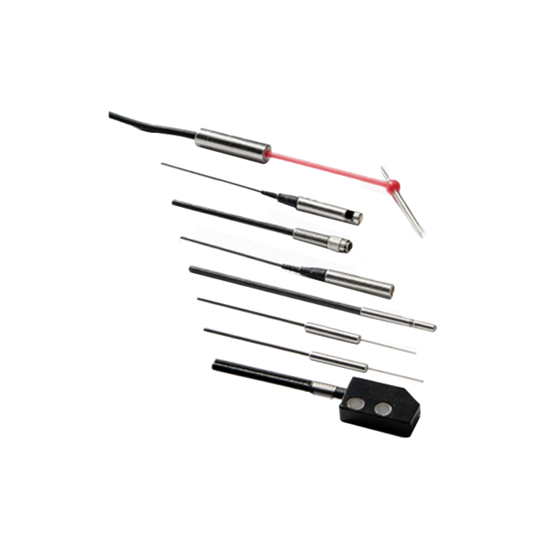
The raw signal from the photodetector is usually weak and noisy. The Amplifier Stage is therefore critical. The schematic for a transimpedance amplifier, common with photodiodes, features an operational amplifier (Op-Amp U1) with a feedback resistor that sets the gain. This stage converts current to voltage while minimizing bandwidth limitations. Following this, additional operational amplifiers may be configured as non-inverting or inverting amplifiers (U2) to provide further gain and signal conditioning. Filtering components, such as capacitors in parallel with feedback resistors or in dedicated low-pass filter configurations, are integrated into the schematic here to suppress high-frequency electrical noise and ambient light interference (like 50/60 Hz flicker from mains lighting).
Threshold Comparison and Output Switching
After amplification, the conditioned signal is fed into a Comparator Circuit (U3). This is a fundamental part of the schematic. The comparator compares the processed signal voltage against a preset reference voltage (Vref). This reference is often user-adjustable via a potentiometer, representing the sensitivity setting of the sensor. The schematic shows the comparator with hysteresis, achieved by positive feedback through a resistor, which prevents output oscillation when the input signal is near the threshold. The output of the comparator is a clean digital signal (high or low) that indicates the presence or absence of the target.
Output Interface and Protection Circuits
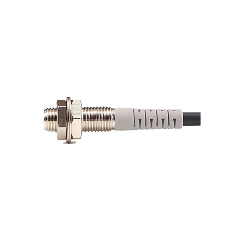
The digital signal from the comparator drives the Output Stage. For a solid-state (PNP or NPN) output, the schematic shows a transistor (Q2) acting as a switch, with necessary base resistors and protection diodes. For relay outputs, a transistor drives the relay coil, with a flyback diode across the coil. For analog or IO-Link sensors, the schematic includes a digital-to-analog converter (DAC) or a communication transceiver chip (U4). Crucially, this section of the schematic also incorporates Protection Circuits. These include reverse polarity protection diodes, TVS diodes for voltage spikes, and RC snubber networks across inductive loads to protect the sensor's internal electronics from field wiring faults and electromagnetic interference.
Power Supply Regulation and Management
A reliable internal Power Supply is the foundation of stable operation. The input power (e.g., 10-30V DC) enters a regulation and filtering section. The schematic depicts a voltage regulator IC (U5), such as a 78-series linear regulator or a more efficient switching regulator, to provide stable +5V or +3.3V for the analog and digital circuits. Decoupling capacitors of various values (e.g., 100µF electrolytic, 0.1µF ceramic) are placed near each IC's power pins, as shown in the schematic, to filter high and low-frequency noise on the supply rails. This clean, regulated power is distributed to the emitter driver, amplifier, comparator, and output stages.
Schematic Variations for Different Sensing Modes
The overall schematic topology adapts based on the sensing mode. A Through-Beam sensor schematic is essentially two separate devices: an emitter unit with its driver circuit and a receiver unit with the full amplification and comparison chain. A Retroreflective sensor schematic integrates emitter and receiver in one housing, with the receiver circuit tuned to detect the specific modulated frequency of its own emitter, ignoring ambient light. The most complex is the Diffuse (Proximity) mode schematic. Here, the receiver must detect light reflected directly from the target. This requires sophisticated circuitry to overcome the enormous dynamic range between the internal optical crosstalk (when no target is present) and the weak return signal from a distant or low-reflectivity target. Advanced schematics may include automatic gain control (AGC) circuits or sophisticated digital signal processing (DSP) blocks.