Introduction to SMD IC Photoelectric Sensors
SMD IC photoelectric sensors represent a significant evolution in sensing technology, integrating the photodetector, signal processing circuitry, and often the light emitter into a single, compact surface-mount device (SMD). These components are fundamental in modern electronics, enabling non-contact detection of objects, distance, color, and ambient light. Their miniaturized form factor, driven by integrated circuit (IC) packaging, makes them ideal for high-density PCB assemblies in consumer electronics, industrial automation, and automotive systems. The core principle involves converting light signals into electrical signals. An internal light source, typically an LED or laser diode, emits light. The photodetector, such as a phototransistor or photodiode, then measures the reflected or transmitted light. The integrated IC amplifies, filters, and processes this signal to provide a clean, digital, or analog output.
Core Technology and Working Principles
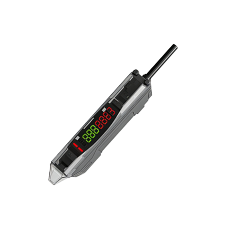
The operational heart of an SMD photoelectric sensor IC lies in its sophisticated internal architecture. Key configurations include through-beam, retro-reflective, and diffuse reflective modes, all achievable within compact modules. In the diffuse reflective type, common in SMD packages, the emitter and receiver are housed together. The IC measures the intensity of light reflected directly from the target object. Advanced versions incorporate modulation techniques, where the emitted light is pulsed at a specific frequency. The IC is tuned to this frequency, making the sensor highly immune to ambient light interference from sources like sunlight or room lighting. This allows for reliable operation in challenging environments. Furthermore, modern ICs integrate ambient light rejection circuits, automatic gain control, and temperature compensation, ensuring stable performance across varying conditions.
Key Advantages of the SMD Format
The transition to Surface-Mount Device packaging offers compelling benefits. First is the dramatic reduction in size and weight, enabling integration into increasingly slim and portable devices like smartphones, tablets, and wearables. Second, SMD components are designed for automated pick-and-place assembly, significantly lowering manufacturing costs and improving production throughput and consistency. They offer superior mechanical stability on the PCB compared to through-hole components. Electrically, the short internal lead lengths minimize parasitic inductance and capacitance, which can enhance high-frequency response and signal integrity. The hermetic or robust packaging of many SMD photoelectric sensors also provides excellent resistance to moisture, dust, and vibration, meeting the reliability demands of automotive and industrial applications.
Primary Applications Across Industries
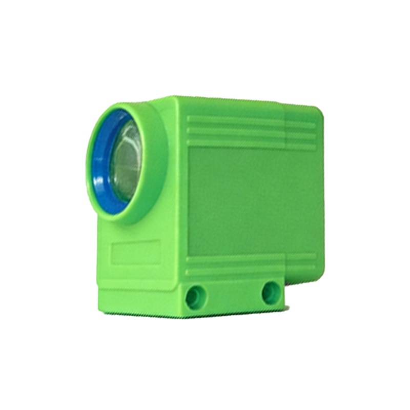
The versatility of SMD IC photoelectric sensors fuels their adoption across diverse sectors. In consumer electronics, they are ubiquitous for display backlight control (ambient light sensors), proximity sensing during phone calls, and automatic brightness adjustment. Industrial automation heavily relies on them for precise object detection on conveyor belts, counting, positioning, and edge guiding in machinery. They form the backbone of optical encoders for motor speed and position feedback. The automotive industry integrates these sensors for rain detection to control automatic wipers, for twilight sensing for headlight control, and in interior systems for occupant detection and gesture recognition. Additionally, they are critical in medical devices for fluid level detection, paper presence in printers, and touchless interfaces.
Critical Parameters for Selection
Selecting the appropriate SMD photoelectric sensor IC requires careful analysis of several technical parameters. Sensing distance and range must match the application, considering the target object's reflectivity. Response time is crucial for high-speed applications like production line counting. The spectral response of the photodetector must align with the emitter's wavelength (common are infrared, red, and green) and the target's properties. Output type is a key decision: digital outputs (open-collector or push-pull) offer simple on/off detection, while analog outputs provide continuous measurement of light intensity or distance. Package size (e.g., 0402, 0603, SOIC) must fit the PCB layout. Engineers must also consider supply voltage range, current consumption, and the sensor's immunity to external optical and electrical noise.
Design Considerations and Integration Challenges
Successful implementation involves more than just component selection. PCB layout is critical; the sensor aperture must have an unobstructed path to the target, which may require cutouts or apertures in the device housing. Careful placement away from other light sources or reflective surfaces prevents crosstalk and false triggering. For sensors with integrated emitters, the drive current must be set correctly via a series resistor to ensure adequate output without degrading LED lifespan. Signal conditioning from the IC's output may still be necessary, such as adding pull-up resistors for open-drain outputs or RC filters for noise suppression. Thermal management is also a factor, as excessive heat from nearby components can affect the sensor's sensitivity and long-term stability.
Future Trends and Developments
The future of SMD IC photoelectric sensors points towards greater intelligence, miniaturization, and multi-functionality. We are seeing the integration of advanced digital interfaces like I2C or SPI, allowing for programmability of parameters such as sensitivity thresholds and output logic. This enables smarter, context-aware sensors. The convergence of sensing modalities is another trend, with combinational sensors that include photoelectric, proximity, and color sensing in one package. There is also a push towards higher precision for tasks like spectral analysis and 3D sensing using time-of-flight (ToF) principles in compact SMD modules. As the Internet of Things (IoT) expands, these sensors will become even more critical, providing essential environmental and positional data to connected devices with minimal power and space requirements.