Early Discoveries and Fundamental Principles
The story of the photoelectric sensor begins not on a factory floor, but in the quiet laboratories of 19th-century physicists. The foundational principle, the photoelectric effect, was first observed by Heinrich Hertz in 1887. While experimenting with electromagnetic waves, Hertz noticed that ultraviolet light facilitated spark generation between electrodes. This curious phenomenon was later meticulously studied by scientists like Philipp Lenard. However, it was Albert Einstein who, in his groundbreaking 1905 paper, provided the correct theoretical explanation, positing that light consists of quanta (photons) whose energy can be transferred to electrons in a material, ejecting them. This theoretical work, which later earned Einstein the Nobel Prize, laid the absolute groundwork for all subsequent photoelectric technology. It established the core concept: light could be converted into an electrical signal, a principle that would become the heartbeat of industrial automation sensing.
The Birth of the First Practical Devices

The transition from theoretical physics to practical engineering took several decades. The invention of the phototube, or photocell, in the early 20th century marked the first major leap. These vacuum tube devices contained a photosensitive cathode. When light photons struck this cathode, they would emit electrons, which were then collected by an anode, generating a small electric current proportional to the light intensity. These early phototubes found their first significant applications not in industry, but in cinema and sound reproduction, notably in reading optical soundtracks on film. Their reliability compared to purely mechanical methods was revolutionary. By the 1930s and 1940s, refinements led to more sensitive and robust designs, paving the way for their initial forays into industrial control, primarily for simple counting and basic safety curtains, though their size, fragility, and power requirements limited widespread adoption.
The Semiconductor Revolution: Enter the Phototransistor and Photodiode
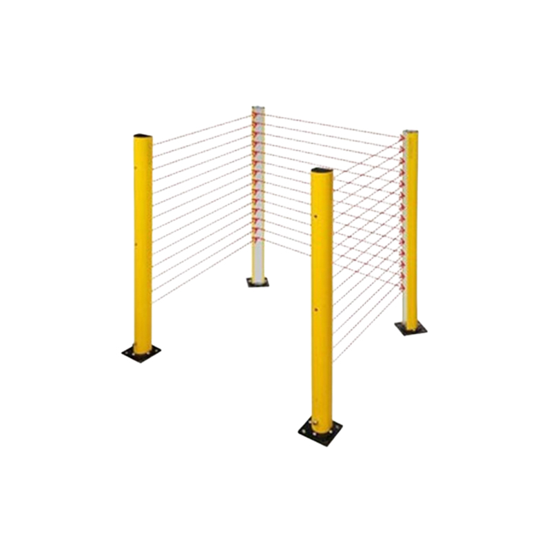
The true democratization of photoelectric sensing began with the advent of semiconductor technology in the 1950s and 1960s. The development of the phototransistor and the photodiode was a paradigm shift. Unlike their vacuum tube predecessors, these solid-state devices were small, rugged, required low voltage, and were amenable to mass production. The photodiode, operating in either photovoltaic or photoconductive mode, offered high speed and linear response. The phototransistor provided built-in signal amplification, delivering a much stronger output signal from the same light input. This era saw the birth of the first recognizable modern photoelectric sensors. They began to be packaged with integrated light sources (initially incandescent bulbs) and basic optics, creating self-contained, reliable units that could detect the presence or absence of an object by sensing the interruption or reflection of a light beam.
The Laser and LED: Enhancing Precision and Reliability
The light source itself became a critical area of innovation. Early sensors used incandescent lamps, which were inefficient, generated heat, had short lifespans, and emitted broad-spectrum light prone to interference. The introduction of the Light Emitting Diode (LED) in the 1970s changed everything. LEDs were solid-state, cool-running, incredibly long-lasting (tens of thousands of hours), and could be engineered to emit very specific wavelengths—red, then later green, and eventually infrared. This allowed for tailored solutions; for example, infrared LEDs became standard for dirt-resistant applications. Shortly after, the laser diode emerged, providing an intense, coherent, and highly collimated beam. This enabled new sensing modes, particularly the precise measurement of very small objects or detection over extremely long ranges with a tight, visible beam spot, revolutionizing positioning and alignment tasks.
Microprocessor Integration and Smart Sensing
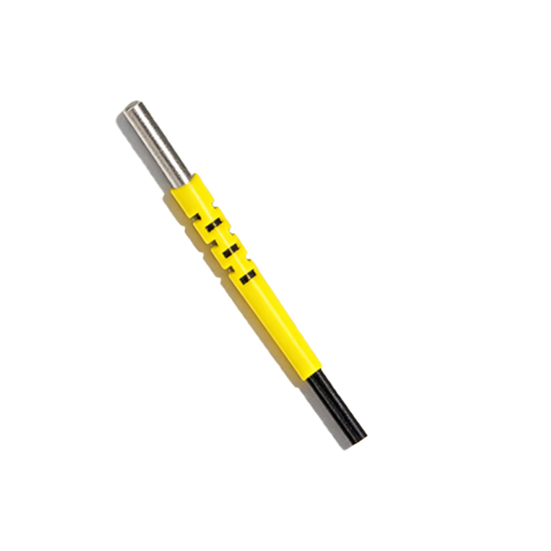
The incorporation of microprocessors and advanced integrated circuits from the 1980s onward transformed photoelectric sensors from simple switches into intelligent devices. This "smart sensor" era introduced features like programmable logic, adjustable sensing thresholds, timers, and counters built directly into the sensor housing. Teach-in functionality allowed for easy setup by simply presenting the target under desired conditions. Advanced background suppression techniques, true color sensing, and the ability to output analog signals (4-20 mA, 0-10V) proportional to distance or reflectivity became possible. Diagnostics, such as built-in signal strength indicators (via LED bargraphs or serial communication), empowered maintenance personnel to troubleshoot and optimize systems proactively, drastically reducing downtime.
Modern Advancements and Future Trends
Today's photoelectric sensors are marvels of miniaturization and connectivity. The development of CMOS and CCD array technology has enabled vision sensor capabilities in compact formats. Sensors now routinely feature robust industrial communication protocols like IO-Link, which provides detailed parameterization, condition monitoring, and seamless integration into Industry 4.0 and IIoT (Industrial Internet of Things) frameworks. This allows for predictive maintenance and data collection from the sensor level. Furthermore, advancements in housing materials (e.g., chemical-resistant PTFE) and optical designs have made sensors incredibly resilient in harsh environments involving extreme temperatures, washdowns, or exposure to oils and solvents. Looking forward, trends point toward even greater miniaturization, higher-speed sensing for robotics, enhanced spectral analysis capabilities, and deeper artificial intelligence integration for pattern recognition and adaptive decision-making directly at the edge of the network.