Introduction to Photoelectric Sensors
Photoelectric sensors are pivotal components in modern industrial automation, robotics, and IoT systems. These devices operate by emitting a light beam—typically infrared, visible, or laser—and detecting changes in the received light intensity to sense the presence, absence, or distance of objects. The core principle relies on the photoelectric effect, where light photons interact with a semiconductor material to generate an electrical signal. Development boards for photoelectric sensors integrate these sensors with microcontrollers, signal conditioning circuits, and communication interfaces, enabling engineers to prototype and test applications efficiently. From simple object detection to complex ambient light sensing, these boards serve as essential tools for innovation in smart manufacturing, automotive safety, and consumer electronics. Their versatility allows for rapid deployment in diverse environments, reducing development time and costs while ensuring reliable performance.
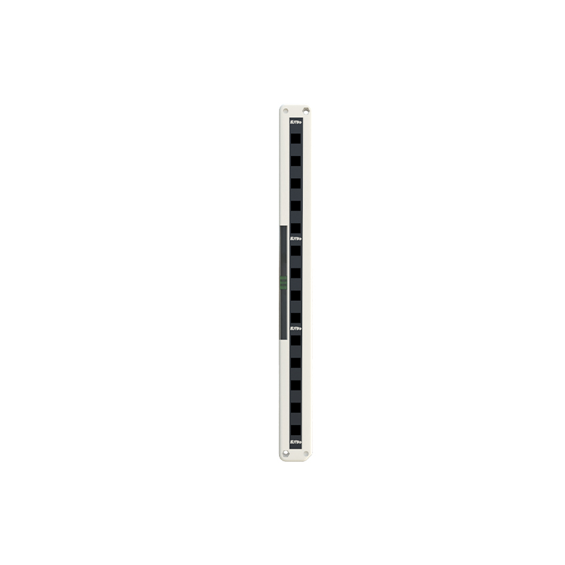
Key Components of a Development Board
A typical photoelectric sensor development board comprises several critical elements. The sensor module itself, such as a phototransistor, photodiode, or integrated ambient light sensor, acts as the primary input device. This is coupled with a microcontroller unit (MCU)—like those from the Arduino, Raspberry Pi, or STM32 families—which processes the analog or digital signals from the sensor. Signal conditioning circuits, including amplifiers, filters, and analog-to-digital converters (ADCs), refine the raw data to improve accuracy and reduce noise. Power management modules ensure stable voltage supply, while communication interfaces like I2C, SPI, UART, or GPIO pins facilitate connectivity with external systems. Additional features may include LEDs for visual feedback, potentiometers for sensitivity adjustment, and prototyping areas for custom circuitry. This modular design empowers engineers to tailor the board to specific needs, from low-power battery-operated devices to high-speed industrial controls.
Applications in Industrial Automation
In industrial settings, photoelectric sensor development boards are indispensable for enhancing efficiency and safety. They enable the creation of systems for object detection on conveyor belts, where sensors monitor product flow and trigger automated sorting or packaging. In quality control, these boards can be programmed to identify defects by analyzing light reflection patterns, ensuring consistent manufacturing standards. For position sensing, they assist in precise alignment of robotic arms or CNC machines, reducing errors and downtime. Environmental monitoring is another key application, with boards detecting dust levels or liquid presence in hazardous areas. By leveraging development boards, engineers can simulate real-world conditions, optimize sensor parameters like range and response time, and integrate with PLCs (Programmable Logic Controllers) for seamless automation. This accelerates the deployment of smart factories, where real-time data from sensors drives predictive maintenance and energy savings.
Design Considerations for Optimal Performance
When working with photoelectric sensor development boards, engineers must account for several design factors to achieve reliable operation. The choice of light source and wavelength is crucial; infrared sensors, for instance, are less affected by ambient light interference, making them suitable for outdoor use. Sensitivity and range should be calibrated based on the target material—shiny or dark surfaces may reflect light differently, requiring adjustable thresholds. Power consumption is a key concern for portable applications, necessitating low-power MCUs and sleep modes. Environmental conditions like temperature, humidity, and dust can impact sensor accuracy, so boards with protective coatings or enclosures are preferred. Signal integrity must be maintained through proper shielding and filtering to mitigate electromagnetic interference (EMI). Additionally, firmware development should include algorithms for debouncing and hysteresis to prevent false triggers. By addressing these aspects during prototyping, engineers can ensure robust performance across varying operational scenarios.
Programming and Integration Techniques
Programming a photoelectric sensor development board involves writing code to interpret sensor data and execute actions. Using platforms like Arduino IDE or STM32Cube, engineers can implement basic routines—such as reading ADC values to detect object proximity—or advanced functions like data logging over Wi-Fi. Libraries for specific sensors simplify development by providing pre-built functions for calibration and communication. Integration with other systems often requires protocol adaptation; for example, I2C can link multiple sensors to a central controller, while UART enables communication with GPS modules or displays. In IoT applications, boards may connect to cloud services via MQTT or HTTP, transmitting sensor data for remote monitoring. Debugging tools, such as serial monitors or oscilloscopes, help identify issues like signal noise or timing errors. By mastering these techniques, engineers can create scalable solutions, from standalone detectors to networked sensor arrays, enhancing interoperability in complex ecosystems.
Future Trends and Innovations
The evolution of photoelectric sensor development boards is driven by advancements in miniaturization, AI, and energy efficiency. Emerging trends include the integration of machine learning algorithms directly on MCUs, enabling boards to perform edge computing for pattern recognition—such as distinguishing between object types without cloud dependency. Ultra-low-power designs, leveraging energy-harvesting technologies, are extending battery life in wireless sensor networks. Enhanced sensitivity sensors, capable of detecting subtle light changes, are opening doors to biomedical applications like heart rate monitoring. Furthermore, the rise of Industry 4.0 is fostering boards with built-in security features and compatibility with 5G networks for real-time data transmission. As materials science progresses, flexible and transparent sensors may become commonplace, allowing integration into wearable devices or smart surfaces. These innovations promise to make development boards more accessible and powerful, fueling next-generation automation and IoT solutions.