Introduction to Micro Proximity Sensor Fundamentals
Micro proximity sensors represent a cornerstone of modern industrial automation and consumer electronics, enabling non-contact detection of objects with exceptional precision. These compact devices operate on various principles, primarily inductive, capacitive, and optical, to sense the presence, absence, or position of a target without physical contact. The core function hinges on the sensor's ability to convert a physical parameter—such as the distance to an object—into a reliable electrical signal. This capability is critical in applications ranging from assembly line robotics and automotive systems to mobile devices and medical equipment. The relentless push towards miniaturization and increased functionality has driven the evolution of their internal architecture, making an understanding of the structural diagram not just academic but essential for effective system integration, troubleshooting, and optimization. A detailed structural breakdown reveals the sophisticated engineering packed into these tiny packages.
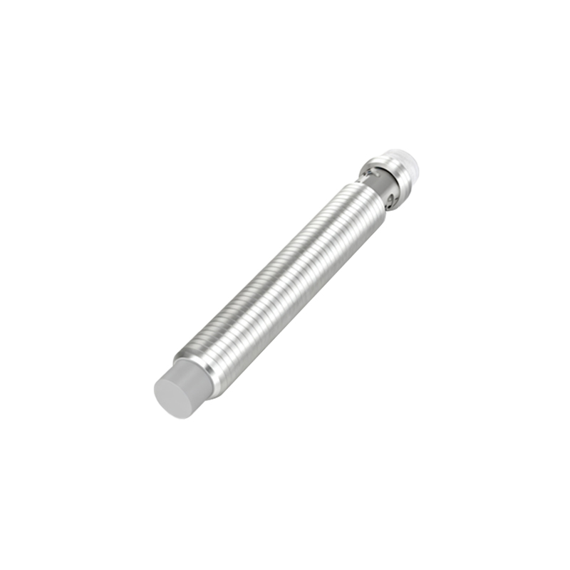
Core Components and Structural Layout
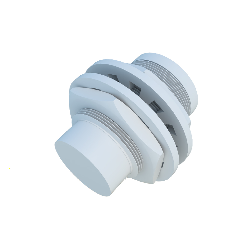
A typical structural diagram of a micro inductive proximity sensor, one of the most common types, can be deconstructed into several key layers and components. At the forefront is the sensing face or active surface, often made of a ferrite core material. Directly behind this is the oscillator coil, the heart of the inductive sensor. This coil generates a high-frequency electromagnetic field that extends from the sensor face. Adjacent to the oscillator is the detection circuit, which continuously monitors the amplitude of the oscillations. When a metallic target enters the sensing field, eddy currents are induced in the target, causing a detectable dampening or attenuation of the oscillator's amplitude. This change is precisely measured by the detection circuit. The signal then passes to a trigger circuit or Schmitt trigger, which provides hysteresis to prevent output chatter and produces a clean, binary switching signal. Finally, the output stage, which can be an NPN/PNP transistor, solid-state relay, or analog amplifier, delivers the usable signal to the connected controller (PLC, microcontroller, etc.). All these components are meticulously arranged on a miniature printed circuit board (PCB) and encapsulated within a robust housing, typically made of nickel-plated brass, stainless steel, or PBT plastic, which provides environmental protection (IP ratings) and electromagnetic shielding.
Detailed Analysis of the Sensing Element
The sensing element's design is paramount to performance. In the structural diagram, the oscillator coil's geometry—its number of windings, diameter, and placement relative to the ferrite core—directly influences the sensor's range, sensitivity, and field shape. The ferrite core serves to concentrate and shape the electromagnetic field, projecting it forward in a defined pattern. For capacitive micro sensors, the diagram would show a different arrangement: electrode plates forming a capacitor. The external target alters the dielectric constant of the surrounding space, changing the capacitance, which is measured by an integrated circuit. Optical micro sensors, another major category, would illustrate an LED light source (infrared or visible), a phototransistor or photodiode receiver, and often a lens system to collimate the light beam. The structural precision here ensures minimal cross-talk, high switching frequency, and immunity to ambient light interference. The diagram highlights how these elements are isolated within the housing to prevent internal signal contamination.
Signal Processing and Output Circuitry
The journey from physical detection to a robust electrical output is managed by the internal signal processing block, a critical section in any structural diagram. Following the detection circuit, the analog signal representing field disturbance is conditioned. This involves amplification to usable voltage levels and filtering to eliminate high-frequency noise inherent in industrial environments. The conditioned signal is fed into a comparator (the Schmitt trigger), which compares it to a predefined reference voltage. Once the signal crosses the "ON" threshold, the output stage is activated. The output stage's architecture is clearly depicted: for a 3-wire DC sensor, it shows the connection of the switching transistor (sourcing or sinking) to the supply voltage and load. Some advanced micro sensors incorporate application-specific integrated circuits (ASICs) that combine the oscillator, detector, and signal conditioner into a single chip, dramatically reducing size and improving reliability. The diagram also indicates protection components like reverse-polarity diodes, surge suppression circuits, and short-circuit protection, which are vital for longevity.
Housing, Integration, and Mounting Considerations
The structural diagram extends beyond the electronics to illustrate the mechanical housing and integration features. The housing is not merely a shell; its design dictates the sensor's mounting style (threaded barrel, rectangular block, slot-style), environmental sealing (IP67, IP69K), and sensing direction (front, side, or top sensing). Diagrams often show O-ring seals, potting compound filling the internal cavity for shock/vibration resistance and moisture protection, and the precise alignment of the sensing face with the housing