Introduction to Analog Photoelectric Sensing
Analog photoelectric sensors are fundamental components in modern industrial automation, providing continuous measurement data for processes such as positioning, edge guiding, and fill-level detection. Unlike their digital counterparts that simply output an on/off signal, analog sensors generate a variable output signal—typically a current (4-20 mA) or voltage (0-10 V)—that is directly proportional to the intensity of the received light. This allows for precise monitoring of distance, transparency, or reflectivity of a target object. The core functionality is derived from a carefully designed electronic schematic that integrates optical components with analog signal conditioning circuitry. This article delves into the schematic principles of these versatile sensors, explaining the key stages from light emission to standardized analog output.
Core Components and Basic Operational Principle
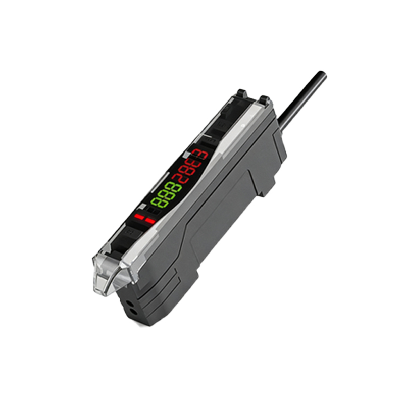
The fundamental schematic of an analog photoelectric sensor comprises three main sections: the transmitter (emitter), the receiver, and the signal processing unit. The transmitter circuit is built around a light-emitting diode (LED), usually infrared, red, or laser, driven by a constant current source to ensure stable light output. The receiver section features a photodiode or phototransistor, which acts as a light-sensitive resistor. Its conductivity changes in relation to the amount of incident light. In a through-beam sensor setup, the emitter and receiver are separate units. In a diffuse-reflective sensor, they are housed together, and the receiver detects light reflected from the target. The received light intensity is inversely proportional to the square of the distance or affected by the target's surface properties, creating the initial analog variation.
Signal Conversion: From Light to Electrical Current
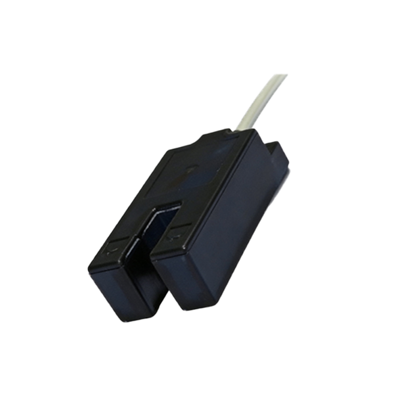
The first critical stage in the schematic is the conversion of light into a minute electrical signal. The photodiode in the receiver is typically operated in photoconductive mode, often with a reverse bias voltage to improve response speed. The incident light generates electron-hole pairs, resulting in a photocurrent (I_PH). This current is extremely small, in the nanoamp or microamp range, and is highly susceptible to noise. Therefore, the schematic immediately employs a transimpedance amplifier (TIA). This operational amplifier (op-amp) circuit converts the weak photocurrent into a more robust proportional voltage. The feedback resistor (R_f) in the TIA sets the gain (V_out = -I_PH * R_f). This stage is meticulously designed with low-noise op-amps and careful PCB layout to maximize the signal-to-noise ratio.
Analog Signal Conditioning and Linearization
The raw voltage from the TIA is not yet suitable for industrial use. It may be non-linear relative to the measured parameter (e.g., distance). The signal conditioning stage involves further amplification, filtering, and often linearization. A programmable gain amplifier (PGA) or a second op-amp stage adjusts the signal to an optimal range for the analog-to-digital converter (ADC). Active low-pass filters are integrated to suppress high-frequency electrical noise and ambient light interference, such as from 50/60 Hz mains lighting. For sensors measuring distance via triangulation in diffuse mode, the signal's relationship to distance is inherently non-linear. A microcontroller (MCU) or a dedicated analog linearization circuit is used to apply a correction algorithm, ensuring the final output signal is linear over the sensor's specified sensing range.
Output Stage: Standardized Analog Interfaces
The conditioned analog signal is finally converted into a standardized industrial output. In modern analog sensors, a high-resolution ADC within the MCU digitizes the voltage for processing. The MCU then drives an output stage that regenerates a clean, load-independent analog signal. The most common outputs are analog voltage (e.g., 0-10V) and analog current (4-20mA). The 4-20mA current loop output is particularly prized for its high noise immunity over long cable runs. The schematic for this stage includes precision voltage references, digital-to-analog converters (DAC), and robust output driver circuits capable of sourcing the required current into the load. This stage often includes protection against short-circuits, overvoltage, and reverse polarity.
Considerations for Schematic Design and Stability
Designing a reliable analog photoelectric sensor schematic requires addressing several key challenges. Temperature compensation is crucial, as both the LED's light output and the photodiode's sensitivity drift with temperature. This is mitigated by using temperature sensors and compensation algorithms in the MCU, or by using feedback loops in the LED driver circuit. Stability of the light source is maintained using constant current drivers with feedback from a monitor photodiode sometimes integrated within the LED package. Power supply regulation is also vital; clean, stable voltage rails are necessary for all active components, especially the sensitive front-end amplifier. Proper shielding and grounding in the schematic layout are essential to prevent electromagnetic interference (EMI) from corrupting the low-level analog signals.
Application-Specific Schematic Variations
The basic schematic adapts to different sensing modes. For a contrast sensor detecting mark/background differences, the circuit is optimized for high-speed response and may include a peak-hold circuit to capture the signal amplitude. For a luminescence sensor, the receiver includes an optical filter to block the excitation wavelength, and the schematic is tuned for extremely low-light detection. In laser-based analog sensors for high-precision measurement, the schematic incorporates drivers for laser diodes and more complex optics, requiring even greater attention to noise reduction and thermal management. Understanding these variations allows engineers to select or design the appropriate sensor for specific application requirements, balancing factors like resolution, response time, and environmental robustness.