Introduction to Proximity Sensing and Semiconductor Integration
Proximity sensing, the ability to detect the presence, absence, or position of an object without physical contact, is a cornerstone of modern industrial automation. While various technologies like inductive, capacitive, and photoelectric sensors exist, the integration of semiconductor technology has revolutionized this field. Semiconductor-based proximity sensors, particularly those utilizing Hall-effect or magnetoresistive elements, offer unparalleled precision, miniaturization, and reliability. Customizing these semiconductor sensors allows engineers to tailor performance characteristics—such as sensing range, response time, power consumption, and output interface—to meet the exacting demands of specific applications, from robotic end-effectors to high-speed packaging machinery.
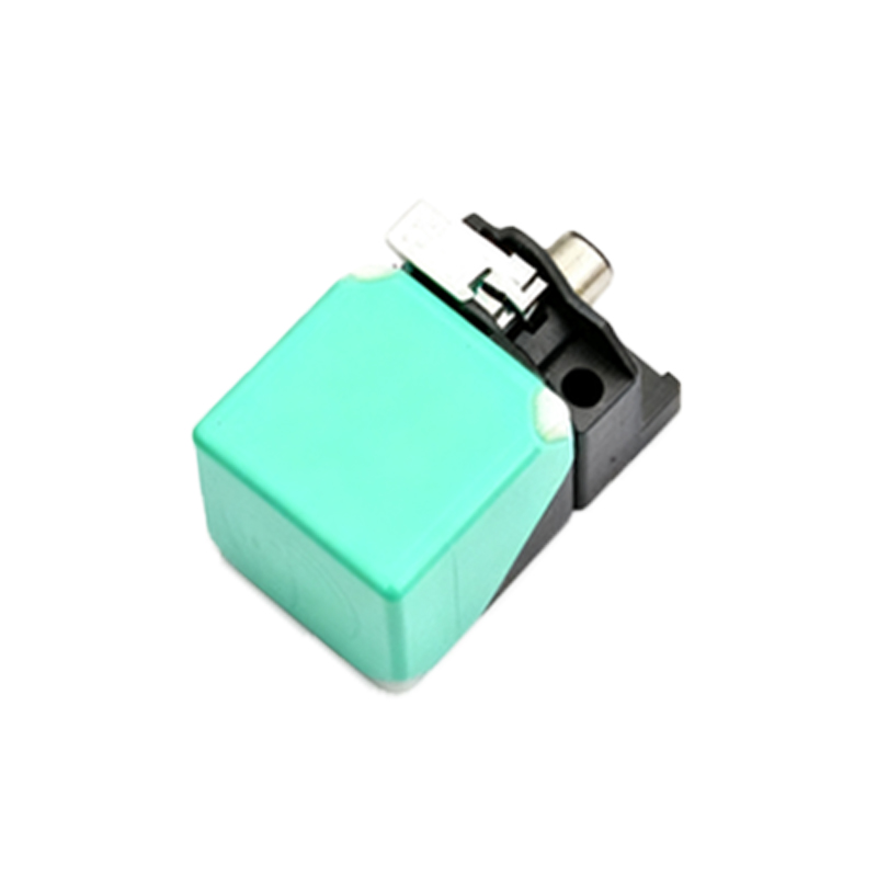
Core Semiconductor Technologies for Custom Proximity Solutions
The heart of a custom semiconductor proximity sensor lies in its sensing element. Hall-effect ICs are predominant, generating a voltage proportional to an applied magnetic field, ideal for detecting permanent magnets or ferrous targets. For higher sensitivity and resolution, anisotropic magnetoresistive (AMR) or giant magnetoresistive (GMR) chips are employed. These technologies enable the detection of extremely subtle magnetic field changes. Beyond the sensing element, customization involves integrating signal conditioning circuitry—amplifiers, comparators, and analog-to-digital converters—directly onto the same silicon die. This System-on-Chip (SoC) approach enhances noise immunity, reduces component count, and allows for the implementation of sophisticated digital features like programmable thresholds and I2C/SPI communication protocols.
Key Design Parameters in Custom Sensor Development
Developing a custom semiconductor proximity sensor is a meticulous process defined by several critical parameters. The operating distance or range is paramount and is influenced by the magnet strength (for magnetic sensing) and the sensitivity of the IC. Response time, often in the microsecond range for semiconductors, must be optimized for high-speed automation cycles. The environmental specification is rigorous; sensors may require customization for extreme temperatures, resistance to vibration, shock, and protection against contaminants like oils or coolants (often specified by IP ratings). Furthermore, the output type—whether a simple PNP/NPN switch, a push-pull signal, a PWM output, or a fully digital bus interface—is a fundamental customization choice dictated by the host controller.
The Customization Workflow: From Concept to Production
A successful customization project follows a structured engineering workflow. It begins with a detailed application requirement analysis, defining all operational and environmental constraints. Sensor specialists then engage in mechanical design, determining the optimal packaging to house the semiconductor die, which could be a tubular housing, a block shape, or an ultra-miniature surface-mount device. Electrical design focuses on the integrated circuit's functionality, ensuring it meets the required sensing logic, output drive capability, and protection against reverse polarity or short circuits. Prototyping and rigorous validation under simulated real-world conditions are crucial steps before finalizing the design for volume production, ensuring long-term reliability and performance consistency.
Application-Specific Customization Examples
The value of customization is best illustrated through real-world applications. In automotive braking systems, custom Hall-effect sensors monitor pedal position with fail-safe accuracy and must operate across a -40°C to 150°C temperature range. For battery-powered handheld tools, the primary driver is ultra-low power consumption, requiring sensors with sophisticated sleep/wake modes integrated into the IC. In collaborative robotics, safety-rated proximity sensors need redundant outputs and built-in self-test functions certified to standards like ISO 13849. Each scenario demands a unique combination of semiconductor technology, packaging, and firmware logic that only a tailored approach can provide efficiently.
Overcoming Challenges in Sensor Customization
Customization is not without its challenges. Electromagnetic interference (EMI) in industrial settings can disrupt sensitive semiconductor signals, necessitating careful PCB layout and shielding strategies within the custom package. Achieving a precise and stable sensing range often involves managing magnetic field gradients and compensating for temperature drift through on-chip algorithms. Cost optimization for medium-volume runs requires a balanced approach, potentially using a programmable Application-Specific Standard Product (ASSP) rather than a full custom ASIC. Close collaboration between the customer's engineering team and the sensor manufacturer's application experts is vital to navigate these complexities and arrive at a cost-effective, high-performance solution.
Future Trends and Smart Sensor Integration
The future of custom semiconductor proximity sensors is inextricably linked to the Industrial Internet of Things (IIoT). Next-generation sensors are evolving into intelligent nodes on the network. Customization will increasingly involve embedding microcontrollers with local processing power to enable predictive maintenance analytics, such as monitoring approach patterns to predict machine wear. Integration with wireless communication modules (e.g., Bluetooth Low Energy,