Introduction to Photoelectric Sensing Fundamentals
Photoelectric sensors operate on the principle of converting light signals into electrical signals to detect the presence, absence, or distance of an object. At its core, this technology relies on three key components: an emitter (light source), a receiver (photodetector), and associated signal processing circuitry. The emitter, typically a Light Emitting Diode (LED) or a laser diode, projects a beam of light. The receiver, often a phototransistor, photodiode, or in some advanced applications, a CMOS or CCD array, detects this light. The fundamental chemical and physical interaction occurs within the semiconductor materials of these components. When photons from the emitter strike the receiver's semiconductor junction, they transfer energy to electrons, exciting them from the valence band to the conduction band. This movement of charge carriers—electrons and holes—generates a photocurrent, which is the primary electrical signal. The intensity of this current is directly proportional to the intensity of the incident light, forming the basis for all subsequent detection logic.
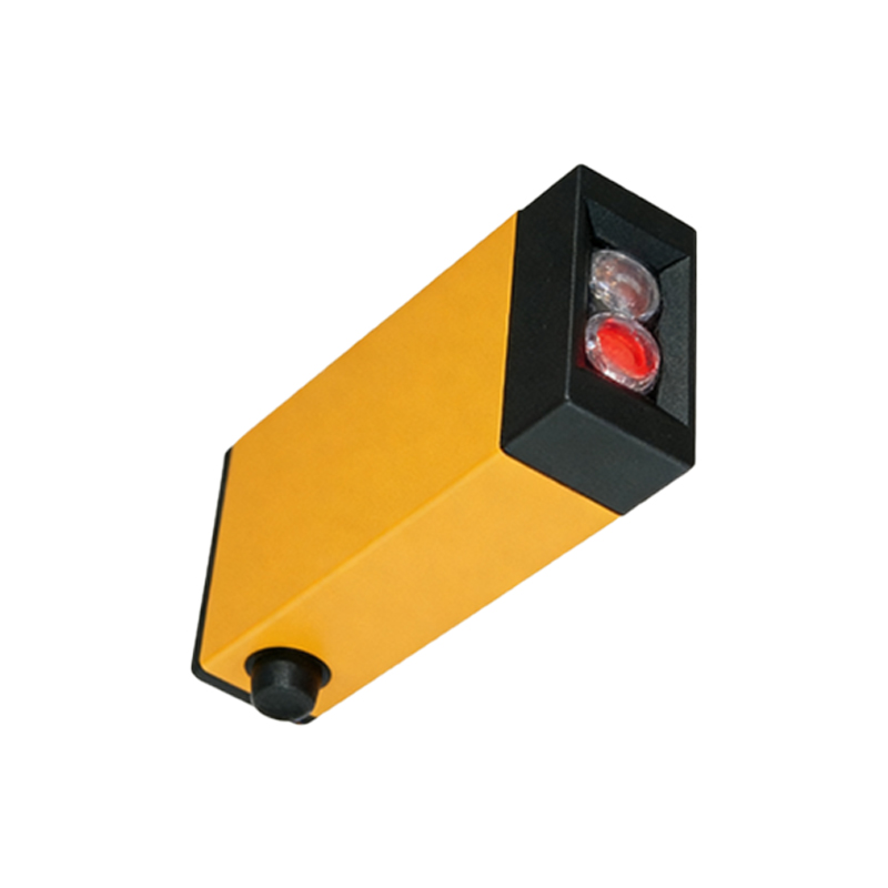
Semiconductor Chemistry in Emitters and Receivers
The chemical composition of the semiconductor materials dictates the sensor's performance characteristics, such as wavelength sensitivity, response time, and temperature stability. Common emitter materials include Gallium Arsenide (GaAs), which emits infrared light around 880-940 nm, and Indium Gallium Nitride (InGaN) for visible light LEDs. The receiver's photodiode or phototransistor is typically made from Silicon (Si) for general-purpose sensing in the visible to near-infrared range, or from Indium Gallium Arsenide (InGaAs) for specialized long-wavelength infrared detection. The doping process, where impurities like Boron (p-type) or Phosphorus (n-type) are introduced into the pure semiconductor crystal lattice, creates the p-n junction. This junction is critical; it establishes an internal electric field that efficiently separates the photon-generated electron-hole pairs, preventing immediate recombination and allowing a usable current to flow. The bandgap energy, a fundamental property determined by the atomic structure and bonding of the semiconductor compound, defines the minimum photon energy (and thus maximum wavelength) that the material can detect or emit.
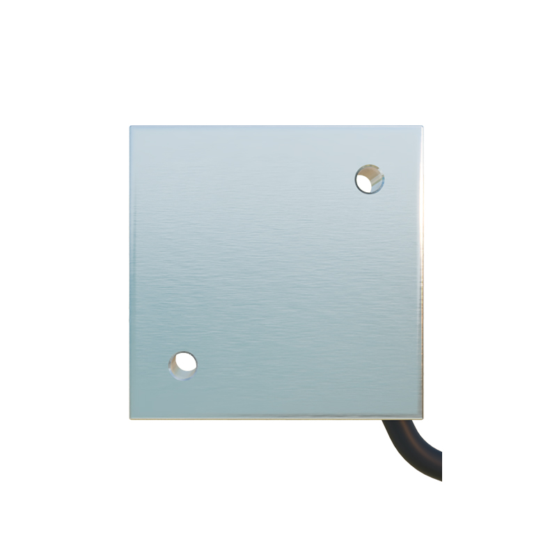
Optical Path and Medium Interaction Principles
The path of the light beam between the emitter and receiver is where the sensor interacts with its environment, which in industrial settings often includes challenging chemical atmospheres. In through-beam, retro-reflective, and diffuse-reflective modes, the light may pass through or reflect off various media. Key principles here include absorption, scattering, and refraction. Molecules in the air or on the target object can absorb specific wavelengths of light according to their molecular structure and bonds. For instance, water vapor (H₂O) and carbon dioxide (CO₂) have strong absorption bands in the infrared spectrum. Advanced sensors often use modulated light at a frequency that avoids these absorption peaks to ensure reliability. Scattering occurs when light collides with particles (dust, smoke, mist), changing its direction. This is governed by the Mie and Rayleigh scattering theories, which depend on particle size and light wavelength. Refraction, governed by Snell's Law, occurs when light crosses the boundary between two media with different refractive indices, such as air and a plastic or glass window protecting the sensor optics.
Signal Processing and Chemical Noise Mitigation
The raw photocurrent from the receiver is weak and susceptible to interference, necessitating sophisticated signal processing. This stage is crucial for distinguishing the true signal from chemical and environmental noise. Amplification circuits, often based on operational amplifiers (op-amps), boost the signal. However, ambient light—a significant noise source—contains photons from various sources (sunlight, fluorescent lamps) that generate a continuous background photocurrent. To counteract this, the emitter's light is typically modulated at a high frequency (e.g., several kHz). The processing circuitry then includes a band-pass filter tuned to this specific frequency. This technique, akin to chemical spectroscopy isolating a specific spectral line, allows the sensor to reject the DC component and low-frequency noise from ambient light. Furthermore, temperature compensation algorithms are employed because the semiconductor's bandgap and the LED's output intensity are temperature-dependent, following the Arrhenius equation's principles, where reaction rates (here, electron transitions) change with thermal energy.
Application-Specific Chemical Considerations and Diagrams
A practical photoelectric sensor diagram for chemical or pharmaceutical applications must account for material compatibility and sensing through specific substances. The diagram would illustrate a sensor with a housing rated for corrosive environments, perhaps made of polyvinylidene fluoride (PVDF) or polytetrafluoroethylene (PTFE). It would show the light path through a sealed window of chemically inert sapphire (Al₂O₃) or fluoropolymer. In applications involving liquid level detection in tanks, the diagram highlights the critical angle for total internal reflection at the interface between the sensor's prism and the air or liquid. The refractive index of the liquid, a physical property determined by its chemical composition and concentration, dictates this angle. For color mark detection, the diagram emphasizes the use of a receiver sensitive to specific wavelengths, leveraging the fact that different dyes and pigments absorb characteristic wavelengths of light, much like a spectrophotometer. The accompanying electronics block diagram would detail the modulation driver, the synchronous demodulator, and the comparator that outputs the final switch signal.
Conclusion and Future Material Trends
Understanding the chemical principles behind photoelectric sensors enables engineers to select the correct type for harsh industrial environments, optimize their performance, and troubleshoot failures related to coating, fogging, or chemical attack on optical surfaces. Future advancements are closely tied to materials science. Emerging materials like organic semiconductors and perovskite crystals offer potential for novel, flexible, or highly sensitive detectors. Quantum dot technology allows for precise tuning of emission and detection wavelengths by controlling the nanocrystal size—a direct application of quantum confinement principles. Furthermore, the integration of micro-electromechanical systems (MEMS) allows for the creation of sophisticated miniaturized optical structures on a silicon chip. As sensor fusion becomes more prevalent, the photoelectric principle will continue to be combined with other sensing modalities, relying on a deep, chemistry-informed understanding of light-matter interaction to create more robust and intelligent industrial automation solutions.