Introduction to Thin-Film Photoelectric Sensors
Thin-film photoelectric sensors represent a significant advancement in optical sensing technology, widely utilized across automation, manufacturing, and robotics. These sensors operate by detecting changes in light intensity, which are converted into electrical signals. The core of their functionality lies in the thin-film semiconductor materials, typically deposited on substrates like glass or silicon. This construction allows for compact, lightweight, and highly responsive devices. Unlike traditional bulky sensors, thin-film variants offer superior integration capabilities, making them ideal for space-constrained applications. Their development stems from the need for more efficient, reliable, and cost-effective sensing solutions in industrial environments, driving innovations in material science and electronic engineering.
Fundamental Working Principles
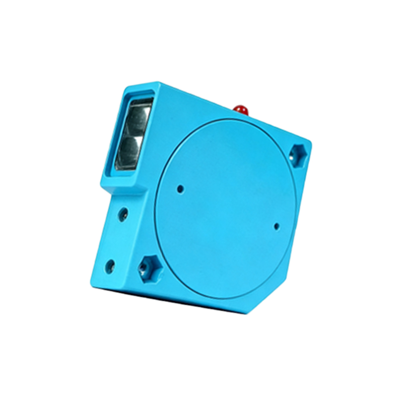
The operation of thin-film photoelectric sensors is based on the photoelectric effect, where light photons striking a semiconductor material generate electron-hole pairs. In thin-film sensors, layers of materials such as amorphous silicon, cadmium telluride, or organic compounds are used. When light hits the active layer, it excites electrons, creating a measurable current or voltage change. This process involves three main components: an emitter (usually an LED or laser diode), the thin-film detector, and signal processing circuitry. The emitter projects a light beam towards the target; the detector then captures reflected or transmitted light, with variations indicating the presence, absence, or characteristics of an object. Advanced designs incorporate multiple thin layers to enhance sensitivity and reduce noise, ensuring accurate detection even in challenging conditions like low light or high ambient interference.
Key Materials and Fabrication Techniques
Material selection is crucial for sensor performance. Common thin-film materials include hydrogenated amorphous silicon (a-Si:H) for its good photoconductivity and low-temperature deposition, and perovskite compounds for high efficiency. Fabrication typically involves techniques like physical vapor deposition (PVD), chemical vapor deposition (CVD), or sputtering, which allow precise control over film thickness and uniformity. These methods enable the creation of layers as thin as a few nanometers, optimizing light absorption and electrical properties. The substrate choice, such as flexible polymers or rigid glass, also impacts durability and application scope. Innovations in nanotechnology have led to quantum dot thin films, offering tunable spectral responses and improved quantum efficiency, pushing the boundaries of sensor capabilities in terms of speed and resolution.
Types and Configurations
Thin-film photoelectric sensors come in various types, primarily differentiated by their sensing modes: through-beam, retro-reflective, and diffuse reflective. Through-beam sensors consist of separate emitter and receiver units, providing long-range and high-accuracy detection. Retro-reflective types use a reflector to bounce light back to the receiver, suitable for medium distances. Diffuse reflective sensors have the emitter and receiver in one housing, detecting light reflected directly from the target, ideal for close-range applications. Additionally, color sensors and contrast sensors utilize thin-film technology to distinguish hues or material differences based on light reflection spectra. Each configuration leverages the thin-film's rapid response and miniaturized form factor to adapt to specific industrial tasks, from object counting to edge detection.
Advantages Over Conventional Sensors
Thin-film photoelectric sensors offer several advantages. Their slim profile allows installation in tight spaces, while low power consumption enhances energy efficiency. The manufacturing process supports mass production, reducing costs. They exhibit fast response times, often in microseconds, crucial for high-speed automation lines. Enhanced durability comes from solid-state construction with no moving parts, resisting vibration and shock. Furthermore, thin films can be engineered for specific wavelength sensitivities, from ultraviolet to infrared, broadening application versatility. Compared to traditional photodiodes or phototransistors, they provide better signal-to-noise ratios and stability over temperature fluctuations, ensuring reliable performance in harsh industrial environments like foundries or clean rooms.
Industrial Applications and Use Cases
These sensors are integral to modern industry. In automotive manufacturing, they detect part presence on assembly lines or monitor robotic arm positions. Packaging industries use them for label verification, fill level control, and product counting. Electronics assembly relies on them for component placement accuracy and PCB inspection. In renewable energy, thin-film sensors monitor solar panel alignment and efficiency. They also play roles in safety systems, such as intrusion detection or machine guarding, where they trigger shutdowns if a person enters a hazardous zone. Emerging applications include wearable health devices, where flexible thin films monitor physiological signals, and smart agriculture, for soil moisture sensing. Their adaptability continues to drive innovation across sectors.
Challenges and Future Trends
Despite benefits, challenges exist. Thin-film sensors can be sensitive to environmental factors like dust, moisture, or extreme temperatures, requiring protective housings. Material degradation over time may affect longevity, prompting research into more stable compounds. Calibration needs can increase maintenance efforts. Looking ahead, trends point toward integration with IoT and Industry 4.0, enabling smart sensors with wireless connectivity for real-time data analytics. Advances in organic thin films and 2D materials like graphene promise higher flexibility and transparency, opening doors to novel applications in displays or biomedical imaging. Additionally, machine learning algorithms are being developed to enhance sensor data interpretation, improving accuracy and predictive maintenance capabilities in complex industrial systems.