Introduction to Photoelectric Sensor Acquisition Chips
At the heart of countless automated systems lies a critical, yet often unseen, component: the photoelectric sensor acquisition chip. This specialized integrated circuit serves as the intelligent interface between the physical world of light detection and the digital realm of control systems. It is responsible for converting the minute analog signals generated by photodiodes or phototransistors into clean, reliable, and processable digital data. Unlike a simple amplifier, a modern acquisition chip integrates signal conditioning, analog-to-digital conversion, and often digital communication protocols into a single, robust package. This integration is fundamental for achieving the high precision, speed, and noise immunity required in demanding industrial environments, from high-speed bottling lines to precise robotic assembly cells.
Core Architectural Components and Functionality
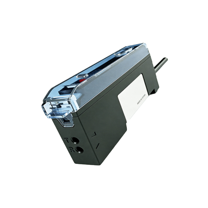
The architecture of a photoelectric sensor acquisition chip is meticulously designed to handle weak signals in electrically noisy surroundings. The signal chain typically begins with a transimpedance amplifier (TIA), which converts the photodetector's current output into a stable voltage. Following this, programmable gain amplifiers (PGAs) allow the system to adapt to a wide range of light intensities without saturation. A high-resolution Analog-to-Digital Converter (ADC), often a sigma-delta type for its excellent noise rejection, digitizes the conditioned signal. Crucially, advanced filtering circuits—both analog and digital—are embedded to suppress ambient light interference, electromagnetic noise, and power supply fluctuations. Modern chips also incorporate diagnostic functions, such as LED health monitoring and fault detection, enhancing system reliability and predictive maintenance capabilities.
Key Performance Parameters for Industrial Selection
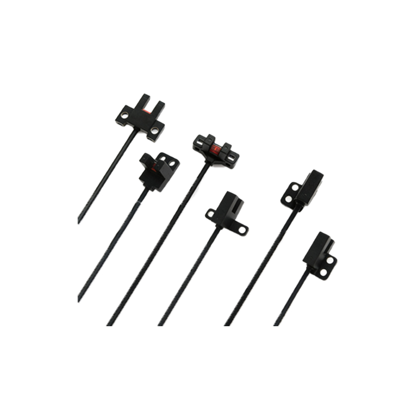
Selecting the appropriate acquisition chip demands careful evaluation of several key parameters. Resolution and sampling rate are paramount; a 16-bit or higher ADC resolution enables detection of extremely subtle changes in light intensity, while a high sampling rate is essential for sensing fast-moving objects. Response time, the delay between a sensing event and a valid output, must be minimized for high-speed applications. Another critical factor is the signal-to-noise ratio (SNR), which determines the chip's ability to distinguish the true signal from background noise. Operating voltage range and power consumption are also vital, especially for portable or battery-operated sensors. Finally, robustness against environmental factors like temperature drift and voltage spikes is non-negotiable for industrial-grade components.
Communication Protocols and System Integration
To function within a larger automation ecosystem, the acquisition chip must communicate effectively. While traditional analog voltage or current outputs (0-10V, 4-20mA) are still common, digital interfaces are becoming the standard. Integrated serial interfaces like I2C, SPI, and UART allow for direct microcontroller connection, enabling configuration of parameters like gain, threshold, and filter settings. For higher-level system integration, industrial fieldbus protocols are increasingly integrated directly onto the chip or through companion ICs. Protocols such as IO-Link are particularly transformative, turning a simple sensor into an intelligent device that can transmit detailed process data, diagnostic information, and parameter sets, facilitating Industry 4.0 and IIoT implementations.
Application-Specific Design Considerations
The application dictates specific chip requirements. For diffuse reflective sensors detecting object presence, chips with excellent background suppression algorithms are key. Through-beam sensors, used for precise positioning, benefit from chips with high dynamic range to handle varying signal strengths. Color recognition sensors require chips capable of processing multiple spectral channels simultaneously. In safety-critical light curtains, ultra-fast response times and redundant circuitry are integrated to meet stringent safety standards (e.g., IEC 61496). Furthermore, chips designed for harsh environments incorporate features like wide temperature operation (-40°C to 125°C) and conformal coating compatibility to withstand moisture, dust, and chemicals.
Future Trends and Technological Advancements
The evolution of photoelectric sensor acquisition chips is driven by the demands of smarter, more connected factories. Future trends point toward even higher levels of integration, combining the photodetector, acquisition circuitry, and a microcontroller core into a single System-in-Package (SiP). Artificial intelligence and machine learning capabilities are beginning to migrate to the edge, with chips featuring embedded neural processing units for on-chip decision-making, such as classifying object types or predicting maintenance needs. Advancements in low-power design will fuel the growth of wireless and energy-harvesting sensors. Simultaneously, the push for miniaturization continues, enabling new sensor form factors for increasingly compact machinery and collaborative robots.