Introduction to Photoelectric Displacement Sensing
Photoelectric sensors have become a cornerstone technology for precise, non-contact displacement measurement across numerous industrial and scientific fields. Unlike mechanical probes or potentiometers, these sensors measure the change in position of an object by detecting variations in light properties, offering significant advantages such as high speed, exceptional accuracy, and no physical wear on the target. The fundamental principle involves projecting a beam of light—often from an LED or laser diode—onto a target surface. The reflected or interrupted light is then captured by a photodetector, such as a photodiode or position-sensitive device (PSD). The electrical signal generated by this photodetector changes in a predictable way as the target moves, allowing the sensor's internal electronics or an external controller to calculate the exact displacement. This method is invaluable for applications requiring real-time feedback on position, vibration, or dimensional changes without physical contact, which could otherwise distort the measurement or damage delicate components.
Core Operating Principles and Sensor Types
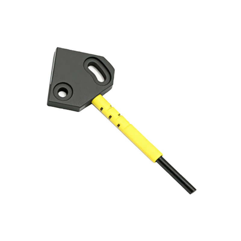
The measurement of displacement using photoelectric technology primarily relies on three distinct principles, each suited to different ranges and accuracy requirements. The first is the triangulation method, commonly used in laser displacement sensors. Here, a focused laser spot is projected onto the target. The reflected light is received by a receiving lens at a specific angle and focused onto a PSD or CMOS/CCD array. As the target distance changes, the position of the reflected spot on the detector shifts linearly. By precisely calculating this spot movement, the sensor determines the displacement with micron-level resolution. The second principle is based on light intensity modulation. In a simple through-beam or reflective sensor setup, the amount of light received by the detector decreases as an object moves into the beam path. While less precise for absolute distance, this method is excellent for detecting presence or measuring displacement within a very limited range where the intensity change is highly predictable. The third principle involves interferometry, typically using laser light. This high-precision technique measures displacement by analyzing the interference pattern created between a reference laser beam and a beam reflected from the target. Changes in the pattern, caused by the Doppler effect or path length variation, correspond to minute displacements, often at the nanometer scale, making it essential for metrology and semiconductor fabrication.
Key Components and Signal Processing
A photoelectric displacement sensor is a sophisticated system comprising several critical components. The light source, typically a red or blue laser diode for high precision or an infrared LED for cost-effective solutions, must provide stable, collimated output. The optics, including projection and receiving lenses, shape the beam and focus the reflected light. The heart of the system is the photodetector. For triangulation sensors, a one-dimensional or two-dimensional PSD or a CMOS linear image sensor is used. The PSD outputs analog currents that indicate the centroid of the light spot, allowing for very fast response. CMOS arrays provide digital pixel data, enabling more complex processing to handle different surface textures. The signal processing circuitry then converts the raw detector signal into a usable displacement value. This involves amplification, filtering to remove ambient light noise, and analog-to-digital conversion. Advanced sensors employ microprocessors to execute algorithms that compensate for factors like target surface color, tilt, and material, ensuring stable and accurate readings. The final output is usually provided as an analog voltage (e.g., 0-10V), current (4-20mA), or digital signal (via Ethernet, IO-Link, or RS-232).
Practical Application Considerations
Selecting and applying the right photoelectric displacement sensor requires careful consideration of several parameters. The measuring range defines the minimum and maximum distances over which the sensor can operate accurately. Resolution, the smallest detectable change in position, is crucial for high-precision tasks. Linearity error indicates how much the sensor's output deviates from a perfect straight line across its range. The target's properties profoundly affect performance; a rough, matte surface scatters light diffusely, while a smooth, shiny surface creates a sharp specular reflection. Sensors often have modes to handle both. Environmental factors like ambient light, temperature fluctuations, dust, and vibrations must be mitigated, possibly requiring sensors with robust housings (IP67 ratings), specialized filters, or temperature compensation circuits. Common industrial applications include monitoring the thickness of rolled metals or plastics, checking the runout and vibration of rotating shafts, controlling the gap in precision assembly robots, and inspecting wafer flatness in cleanrooms. The non-contact nature also makes these sensors ideal for measuring hot, soft, or fast-moving objects.
Advantages, Limitations, and Future Trends
The advantages of photoelectric displacement sensors are compelling. They enable high-speed measurement, often in the kilohertz range, which is impossible for contacting probes. The absence of physical contact eliminates hysteresis, mechanical wear, and measurement force that could deform soft targets. They offer very high resolution and repeatability. However, limitations exist. Performance can degrade with optically challenging surfaces like transparent glass or deeply uneven textures. Ambient light interference, though often filtered, can be an issue in uncontrolled environments. High-precision models, especially laser-based ones, can be costly. Looking forward, trends are pushing the boundaries of this technology. The integration of smarter onboard processing with AI algorithms allows sensors to self-adapt to different surface conditions. Miniaturization is enabling integration into smaller devices and MEMS systems. Furthermore, the development of multi-point and profile sensors, which use array detectors to measure an entire line or area at once, is expanding applications into 3D contouring and complex shape analysis, solidifying the role of photoelectric sensing as a versatile and indispensable tool in advanced automation and quality control.