The Dawn of Photoelectric Sensing
The story of photoelectric sensor development begins not with a single invention, but with the foundational discovery of the photoelectric effect. In the late 19th and early 20th centuries, scientists like Heinrich Hertz and Albert Einstein laid the theoretical groundwork. Einstein's 1905 paper, for which he later won the Nobel Prize, explained that light could eject electrons from a material. This principle became the cornerstone. Early applications were crude, often limited to laboratory experiments and simple light detection. The first commercial devices emerged in the mid-20th century, utilizing vacuum tubes and primitive photocells. These were bulky, power-hungry, and unreliable, but they proved the concept's potential for industrial automation, sparking the imagination of engineers worldwide.
The Solid-State Revolution
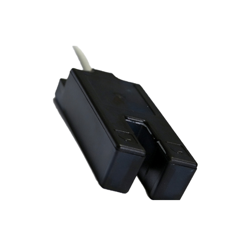
The invention of the transistor and the subsequent development of solid-state electronics in the 1950s and 1960s catalyzed the first major leap. The phototransistor and later the photodiode replaced fragile vacuum tubes. These components were smaller, more robust, and required significantly less power. This era saw the birth of the first recognizable self-contained photoelectric sensors. They typically employed incandescent lamps as light sources and offered basic functions like on/off detection. The introduction of light-emitting diodes (LEDs) in the 1960s was a game-changer. LEDs, particularly infrared LEDs, provided a reliable, long-lasting, and fast light source, enabling more compact and efficient sensor designs. This period established the through-beam, retro-reflective, and diffuse reflective sensing modes that remain standard today.
Integration and Intelligence
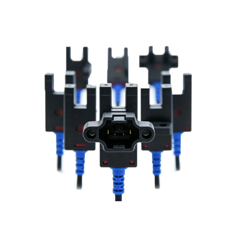
The 1970s and 1980s marked the age of integration and early intelligence. Microprocessors began to find their way into sensor electronics. This allowed for the development of sensors with adjustable sensitivity, time delays, and simple logic functions. Analog output versions (0-10V, 4-20mA) emerged, enabling precise distance or contrast measurement, not just presence detection. The packaging also evolved, with manufacturers offering sensors in standardized, rugged housings with IP67 ratings for harsh industrial environments. Laser diodes started to appear in specialized sensors, providing extremely focused beams for high-precision applications. This era transformed photoelectric sensors from simple switches into versatile measurement tools.
The Digital and Fiber Optic Advance
The 1990s and early 2000s were defined by digitalization and specialization. Advanced integrated circuits allowed for sophisticated background suppression techniques, teaching functions, and diagnostic capabilities via LED indicators. The widespread adoption of programmable logic controllers (PLCs) drove the demand for sensors with digital communication interfaces. Simultaneously, fiber optic technology became integral. Fiber optic cables, coupled with compact amplifiers, allowed sensing in incredibly tight spaces, extreme temperatures, or areas with high electromagnetic interference. This opened new applications in semiconductor manufacturing, medical devices, and food processing. Sensors became smarter, with the ability to self-monitor lens contamination or signal strength.
The Era of Connectivity and Vision
From the 2010s to the present, the development trajectory has been shaped by Industry 4.0 and the Industrial Internet of Things (IIoT). Modern photoelectric sensors are network nodes. They feature industrial Ethernet protocols (EtherNet/IP, PROFINET, IO-Link) that enable remote configuration, real-time data monitoring, and predictive maintenance. IO-Link, in particular, has revolutionized sensor integration by providing detailed parameterization and rich diagnostic data down to the field level. Furthermore, the lines have blurred between traditional photoelectric sensors and machine vision. "Smart sensors" now incorporate advanced functions like color detection, precise contrast measurement, and even basic shape recognition using CMOS technology and embedded processors. The focus is on providing not just a signal, but actionable data.
Future Frontiers: Miniaturization and AI
The current frontier points toward even greater miniaturization, energy efficiency, and intelligence. The integration of micro-electro-mechanical systems (MEMS) could lead to sensor elements on a chip. Research into new materials and light sources, such as VCSELs (Vertical-Cavity Surface-Emitting Lasers), promises higher performance and new wavelengths. The most significant trend is the nascent integration of artificial intelligence at the edge. Future sensors will likely embed tiny AI algorithms capable of adaptive learning, anomaly detection, and complex decision-making without constant cloud connectivity. This will push photoelectric sensing beyond mere detection into the realm of contextual understanding and autonomous process optimization, solidifying its role as a critical enabler of fully automated, intelligent factories.