Introduction to Photoelectric Sensor Sensing Chips
At the heart of every modern photoelectric sensor lies its sensing chip, a sophisticated semiconductor component that converts light signals into electrical impulses. These chips are engineered to detect the presence, absence, or distance of an object by utilizing a light source, typically an LED or laser diode, and a photodetector integrated into the chip. The fundamental principle involves the emission of a light beam; when this beam is interrupted or reflected by a target object, the photodetector on the chip registers the change in light intensity. This detection triggers a precise electrical output signal. The miniaturization and integration of these optical and electronic elements onto a single chip are feats of microelectronics, enabling sensors to achieve remarkable sensitivity, speed, and reliability in demanding industrial environments. Their role is foundational, acting as the critical interface between the physical event of light interaction and the digital control systems of automation.
Key Technologies and Operating Principles
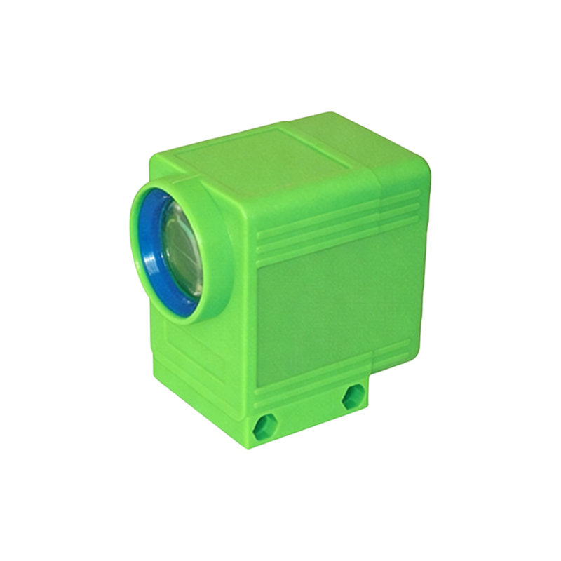
Photoelectric sensor chips operate primarily on three principles: through-beam, retro-reflective, and diffuse reflection. In through-beam mode, the emitter and receiver are on separate chips housed in opposing housings. The sensing chip on the receiver side is designed for high sensitivity to detect the precise interruption of the beam. Retro-reflective chips are calibrated to recognize light reflected from a dedicated reflector, filtering out ambient light interference. The most common and versatile is the diffuse reflection principle, where the emitter and receiver are co-located on or near the same chip module. The chip's photodetector is finely tuned to detect light scattered back from the target object itself. Advanced chips incorporate background suppression technology, using triangulation or time-of-flight (ToF) measurement integrated into the chip design to measure distance precisely, ignoring objects beyond a set range. This is achieved through specialized pixel arrays and signal-processing circuits embedded within the chip architecture.
Material Science and Chip Fabrication
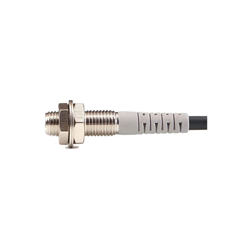
The performance of a sensing chip is dictated by its material composition and fabrication process. The photodetector element is commonly made from silicon (Si) for general-purpose visible and near-infrared light detection. For specific wavelengths, such as in laser-based sensors, materials like indium gallium arsenide (InGaAs) are used. The chip fabrication involves photolithography, etching, and doping processes to create photodiodes, phototransistors, and often accompanying amplification circuits on a tiny silicon wafer. Manufacturers are increasingly integrating Application-Specific Integrated Circuits (ASICs) onto the same die. These ASICs handle signal conditioning, noise reduction, and output switching, which dramatically improves signal integrity, response time (often in microseconds), and immunity to electromagnetic interference (EMI). The packaging of the chip is equally critical, featuring lenses that focus light and protective coatings that ensure long-term stability against dust, moisture, and chemical exposure.
Applications Across Industrial Sectors
The robustness and precision of modern sensing chips have unlocked applications across every industrial sector. In packaging and material handling, chips with high-speed response detect labels, count bottles, and monitor fill levels on high-speed conveyor lines. Automotive assembly lines rely on them for precise part positioning and robot guidance. In electronics manufacturing, miniature chips perform delicate tasks like verifying component placement on printed circuit boards (PCBs). Logistics and warehousing utilize chips in barcode scanners and automated storage/retrieval systems for item tracking. Furthermore, chips with background suppression are indispensable in automated forklifts for pallet detection and in agricultural machinery for crop monitoring. Their ability to function reliably in environments with vibration, temperature fluctuations, and contaminant exposure makes them the default choice for non-contact sensing.
Selection Criteria and Integration Considerations
Selecting the appropriate sensor with the right sensing chip requires careful analysis of several parameters. The sensing range, determined by the chip's sensitivity and lens design, must match the application. The size and reflectivity of the target object influence the choice of chip technology; small, dark, or shiny objects may require a chip with focused beam or polarized lens options. Environmental factors like ambient light, dust, and fog necessitate chips with robust modulation techniques (e.g., pulsed LED light) and high ingress protection (IP) ratings. Electrical output type (PNP/NPN, analog, IO-Link) is defined by the chip's integrated circuitry and must be compatible with the host controller. Engineers must also consider mounting constraints, required response frequency, and connectivity for Industry 4.0 data acquisition, which is increasingly supported by smart chips with digital communication protocols.
Future Trends and Advancements
The evolution of photoelectric sensor chips is driven by the demands of smarter, more connected factories. Future trends point toward greater intelligence at the chip level. We are seeing the integration of microprocessors that enable advanced functions like teach-in capabilities (self-configuration via a button press), condition monitoring (reporting lens contamination or LED aging), and built-in diagnostics directly on the chip. The miniaturization trend continues, allowing sensors to fit into increasingly compact machinery. Furthermore, the convergence of sensing technologies is leading to multi-functional chips that combine photoelectric sensing with other parameters like temperature or humidity. Research into new semiconductor materials and nano-photonics promises chips with even higher sensitivity, lower power consumption, and the ability to detect a broader spectrum of light, paving the way for next-generation industrial automation and IoT applications.