In the world of industrial automation, consumer electronics, and robotics, the humble proximity sensor plays a critical role. While technical specifications and datasheets provide the hard data, high-resolution images of these components offer an unparalleled visual understanding of their design, construction, and application context. This visual guide delves into the world of high-definition proximity sensor imagery, exploring what these pictures reveal and why they are essential for engineers, purchasers, and enthusiasts alike.
A high-resolution image of a proximity sensor is more than just a pretty picture; it is a detailed technical document. The first element that becomes clear is the form factor and physical construction. Crisp, close-up photos allow viewers to distinguish between different housing materials, such as rugged stainless steel for harsh industrial environments or compact plastic housings for consumer devices. You can see the precise machining of threads on cylindrical inductive sensors, the quality of sealing gaskets that provide an IP67 or IP69K rating for water and dust resistance, and the robustness of the sensor body designed to withstand vibration and mechanical shock.
The lens or sensing face is another area where detail matters immensely. In capacitive or photoelectric sensors, the condition and clarity of the lens are paramount. A high-definition image can reveal if the lens is made of glass or specialized plastics, its surface texture, and any protective coatings. For inductive sensors, the image showcases the active sensing surface, often a flat or slightly rounded face from which the electromagnetic field emanates. Scratches, imperfections, or signs of wear that could affect performance are easily identifiable in a high-quality photograph.
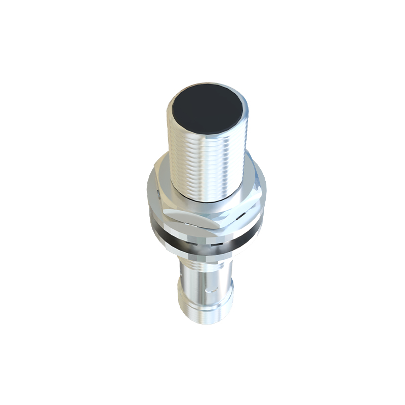
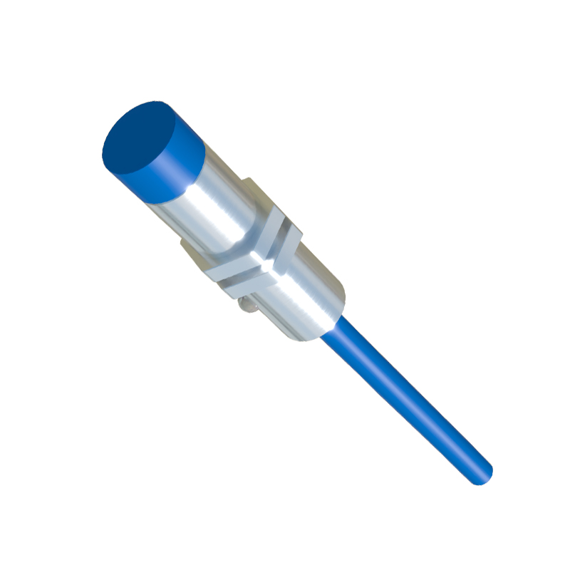
Wiring and connection interfaces are crucial for proper installation. Clear images show the type of electrical connection, whether it's a standard M8 or M12 quick-disconnect connector, a PVC cable outlet, or flying leads. The color coding of wires—brown for DC+, blue for DC-, black for output signal—is distinctly visible, aiding in correct wiring and reducing installation errors. Some detailed shots even include a ruler or common object for scale, providing immediate understanding of the sensor's actual dimensions, which is vital for designing tight spaces in machinery or circuit boards.
Beyond the sensor itself, application photos are incredibly valuable. A high-resolution image showing an inductive proximity sensor mounted on a robotic arm, precisely detecting the position of a metal component on an assembly line, tells a powerful story. It demonstrates the sensor's integration, its relative size in a real-world setting, and the typical gap (the sensing distance) maintained between the sensor and the target. Similarly, a clear photo of a capacitive sensor detecting the fluid level inside a transparent tank, or an infrared sensor counting objects on a conveyor belt, provides immediate context that pages of text cannot.
For optical and ultrasonic sensors, internal component layout can sometimes be inferred from external design, but cutaway or exploded-view images are the gold standard. These high-definition illustrations or photographs reveal the internal arrangement: the LED light source and phototransistor in a photoelectric sensor, the coil and oscillator circuit in an inductive sensor, or the piezoelectric element in an ultrasonic sensor. These visuals demystify the technology, making it accessible for educational purposes and deeper technical analysis.
The demand for such high-quality imagery comes from several sectors. Engineers and machine designers use them for prototyping and integration planning. Procurement specialists rely on them to verify product authenticity and exact model types before purchasing. Educators and students utilize them as learning aids to understand sensor technology without needing physical samples. Furthermore, in marketing and technical documentation, clear, professional photos build trust, showcase product quality, and help users identify replacement parts quickly.
When searching for or creating high-resolution proximity sensor images, focus on key aspects: lighting should be even to avoid glare on metallic or glossy surfaces, especially on lenses. The background should be neutral and uncluttered, typically white or grey, to keep the focus entirely on the sensor. Multiple angles are essential—front, side, rear with connector, and a top-down view. Macro capabilities are needed to capture minute details like part numbers, logos, and tiny electrical contacts.
In conclusion, high-resolution images of proximity sensors serve as a critical bridge between abstract technical data and practical, tangible understanding. They empower professionals to make informed decisions, ensure correct applications, and foster a deeper appreciation for the intricate engineering embedded in these ubiquitous devices. In an increasingly visual and digital world, the clarity provided by a high-definition picture is not just convenient; it is a fundamental tool for innovation and efficiency in technology-driven fields.