CMOS (Complementary Metal-Oxide-Semiconductor) sensors are integral components in modern electrical and imaging systems, widely used in cameras, industrial inspection equipment, and optical measurement devices. However, these sensors are highly vulnerable to damage from laser exposure, a critical concern for engineers designing and maintaining such systems. This article delves into the mechanisms of laser-induced damage, its implications for system reliability, and practical mitigation strategies.
When a laser beam strikes a CMOS sensor, the intense, focused light energy can cause both immediate and cumulative damage. The primary mechanism is thermal: the laser energy is absorbed by the silicon photodiodes and surrounding structures, leading to rapid localized heating. This can melt or vaporize microscopic elements, creating permanent defects. Even lasers with power outputs below visible damage thresholds can cause gradual degradation through phenomena like lattice displacement or dopant diffusion, ultimately reducing sensor sensitivity and increasing noise.
Another significant risk is electrical overstress. CMOS sensors operate with precise voltage levels across their junctions. A high-intensity laser pulse can generate a surge of photocurrent, exceeding the design limits of the transistors and interconnects. This can lead to gate oxide breakdown, junction burnout, or latch-up—a state where the device draws excessive current and may self-destruct. Pulsed lasers, especially those with short nanosecond or picosecond durations, are particularly hazardous as they deliver high peak power even at low average power.
The consequences of such damage in industrial settings are severe. In machine vision systems, a damaged sensor may produce dead pixels, streaks, or complete failure, halting production lines. In scientific or medical imaging, it compromises data integrity. Notably, damage is not always instantly apparent; latent defects can evolve over time, leading to unpredictable failures.

To protect CMOS sensors, engineers employ multiple strategies. Optical filters are the first line of defense. Bandpass or notch filters can block specific laser wavelengths while transmitting desired light. For broad-spectrum protection, neutral density filters attenuate overall light intensity. Physical barriers or shrouds can limit direct exposure in open systems.
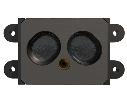
Electronic safeguards are equally important. Integrating automatic gain control (AGC) and exposure limiters in the sensor's driver circuitry can prevent saturation from sudden bright light. Using sensors with built-in anti-blooming technology helps contain charge spillage from overexposed pixels. In critical applications, redundant sensor arrays or periodic calibration checks can identify degradation early.
Furthermore, system design must consider operational environments. In facilities using lasers for cutting, welding, or alignment, ensuring proper beam containment and implementing interlock systems that shut down sensors when laser shields are open is crucial. Training personnel on laser safety protocols around sensitive electronics minimizes accidental exposure.
Material advancements also offer promise. Research into hardened sensor designs, such as those with protective coatings or more robust semiconductor materials, aims to increase laser damage thresholds. However, these often involve trade-offs in cost or performance.
In conclusion, laser damage to CMOS sensors is a multifaceted engineering challenge rooted in thermal and electrical physics. Proactive protection through optical, electronic, and administrative measures is essential to ensure the longevity and reliability of electrical systems incorporating these sensitive components. As laser technology proliferates, understanding and mitigating this risk becomes increasingly vital for maintaining operational integrity across industries.