The genesis of camera-based laser sensors, often termed laser vision sensors or structured light sensors, is a compelling narrative of interdisciplinary convergence. It is a story that begins not with a single eureka moment, but through the parallel evolution of several key technologies: the laser, the solid-state image sensor, and computational processing power. The journey from theoretical concepts to indispensable industrial tools encapsulates decades of innovation aimed at solving the fundamental challenge of non-contact, precise dimensional measurement.
The foundational element, the laser (Light Amplification by Stimulated Emission of Radiation), was first demonstrated in 1960. Its coherent, monochromatic, and highly directional light properties were immediately recognized as revolutionary. Early industrial applications, emerging in the late 1960s and 1970s, primarily utilized lasers for alignment, interferometry for ultra-precise distance measurement, and simple photoelectric detection. These were point-based systems, measuring a single spot. The need for profiling a surface or capturing complex 3D contours required scanning a laser point or projecting a line. The invention and commercialization of laser diodes in the 1970s and 1980s were pivotal, providing a compact, efficient, and reliable light source that could be easily modulated, making robust industrial sensors feasible.
Simultaneously, the imaging world was undergoing its own revolution. The Charge-Coupled Device (CCD), invented in 1969 at Bell Labs, provided a means to capture light electronically in a discrete pixel array. This was a monumental leap from film and vacuum tube cameras. The CCD enabled the conversion of a projected laser line or pattern from an analog optical signal into a digital matrix of intensity values. The subsequent development of the Complementary Metal-Oxide-Semiconductor (CMOS) active-pixel sensor in the 1990s offered lower power consumption and the potential for on-chip processing, further accelerating adoption. The camera was no longer just a recorder of scenes; it became a precise measurement instrument when paired with a calibrated laser source.
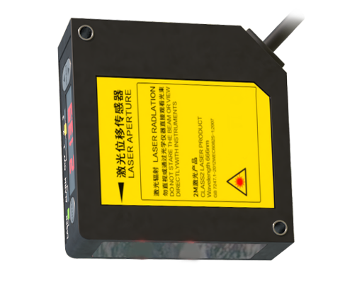
The true birth of the integrated camera-based laser sensor occurred when these two streams merged with the rise of affordable, powerful microprocessors. The core operational principle—triangulation—is geometrically straightforward, but its practical implementation demanded real-time computation. A laser line is projected onto a target object. The camera, positioned at a known angle to the laser projector, views this line. Any deviation in the object's surface height causes the laser line to appear displaced in the camera's image plane. By analyzing the pixel coordinates of this deformed line and applying a calibration matrix that defines the sensor's geometry, a dedicated processor can calculate the precise 3D profile of the object along that line. This is laser line profiling or 2.5D sensing. For full 3D point clouds, techniques like laser scanning or the projection of complex coded light patterns were developed.
The driving force for this integration was unequivocally industrial. The automotive and electronics manufacturing sectors of the 1980s and 1990s faced escalating demands for quality control, robot guidance, and assembly verification. Traditional contact probes on Coordinate Measuring Machines (CMMs) were too slow and fragile for production lines. Non-contact optical methods existed but lacked robustness, speed, or accuracy. Pioneering companies, often spin-offs from academic research in optics and computer vision, began packaging lasers, cameras, and processors into sealed, hardened units. These early systems addressed critical applications: weld seam tracking, where a sensor guided a robot along a joint; part presence and orientation verification; and basic height measurement for tolerance checking.
The evolution since those early integrations has been marked by exponential growth in performance and miniaturization. Key advancements include the development of blue lasers for better performance on shiny or organic materials, high-speed CMOS global shutters that freeze motion, and sophisticated algorithms for sub-pixel edge detection and data filtering. The processing has migrated from external PCs to powerful embedded systems-on-a-chip (SoCs) within the sensor housing. Communication protocols evolved from analog I/O to fieldbuses like Profibus and Ethernet/IP, and now to GigE Vision and USB3 Vision, streamlining integration into larger vision systems.
Today, camera-based laser sensors are a cornerstone of Industry 4.0 and smart factory initiatives. They provide the critical metrology data for closed-loop process control, robotic bin picking, and detailed inline inspection of everything from battery electrodes to pharmaceutical packaging. Their origin story is a testament to solving hard industrial problems through the synthesis of physics (laser optics), electronics (sensors), and computer science (algorithms). From bulky, finicky prototypes to robust, off-the-shelf components, these sensors have fundamentally transformed how industry sees and measures the physical world, enabling levels of automation, quality, and efficiency once thought impossible. Their continued development, now incorporating artificial intelligence for anomaly detection and adaptive measurement, promises to further embed them as the intelligent eyes of modern manufacturing.