In modern industrial automation, laser sensors have become indispensable tools for precision measurement, object detection, and quality control. A laser sensor system integrates optics, electronics, and signal processing to deliver high-accuracy, non-contact sensing capabilities. To fully grasp its functionality, engineers must understand the system block diagram, which breaks down the complex interactions into manageable subsystems. This article provides a detailed exploration of a typical laser sensor system block diagram, explaining each component's role and how they collectively achieve reliable performance.
The core of a laser sensor system begins with the Laser Source Module. This module typically employs a semiconductor laser diode, which emits coherent, monochromatic light at a specific wavelength (common ranges include 635 nm to 1550 nm). The laser source is driven by a constant current driver circuit to ensure stable output power, minimizing fluctuations due to temperature changes or aging. Key parameters here include output power, beam divergence, and wavelength stability, which directly influence the system's range and accuracy.
Next, the Optical Transmission and Conditioning Block shapes and directs the laser beam. This includes collimating lenses to produce a parallel beam, which reduces divergence over distance. For applications requiring precise focusing, additional lenses or optical assemblies are used. In some systems, beam splitters or diffractive optical elements (DOEs) may be incorporated to create structured light patterns, enabling advanced features like 3D profiling. This block ensures the laser is optimally delivered to the target area.
The Target Interaction Zone is where the laser beam meets the object being measured. Depending on the sensing principle—such as triangulation, time-of-flight (ToF), or interferometry—the interaction varies. In a triangulation-based sensor, the laser spot on the target is observed at an angle; in ToF systems, the time delay of reflected light is measured. Environmental factors like surface reflectivity, ambient light, and dust can affect performance, necessitating robust design in subsequent stages.
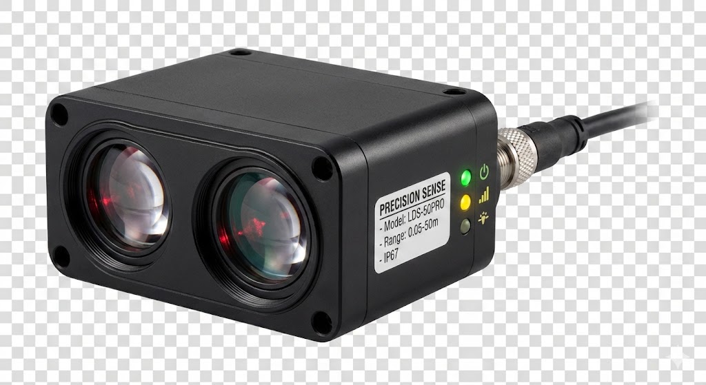
Reflected or scattered light from the target enters the Optical Reception Module. This module features a photodetector, often a photodiode or a position-sensitive device (PSD) for triangulation sensors, or an avalanche photodiode (APD) for ToF systems. The detector converts optical signals into electrical currents. Preceding optics, such as filters (e.g., bandpass filters to block ambient light) and focusing lenses, enhance signal quality by maximizing relevant light capture while minimizing noise.
The Signal Conditioning and Processing Block is critical for extracting meaningful data. The weak electrical signal from the detector is first amplified by a transimpedance amplifier (TIA), which converts current to voltage. Filtering stages (low-pass or band-pass) remove high-frequency noise and interference. For analog systems, this conditioned signal might be directly used; in digital systems, an analog-to-digital converter (ADC) digitizes the signal for further processing. Microcontrollers or digital signal processors (DSPs) then apply algorithms—like peak detection for triangulation or time measurement for ToF—to compute parameters such as distance, displacement, or presence.
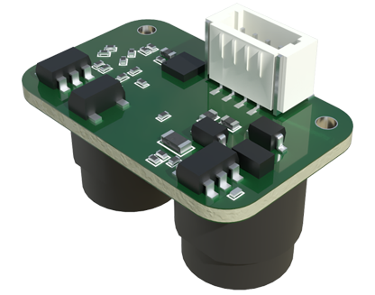
Integration continues with the Control and Interface Block. This includes a central processing unit (CPU) or FPGA that manages system timing, calibrations, and communication protocols. User-configurable settings (e.g., sensitivity thresholds, output formats) are handled here. Output interfaces can be analog (0-10V, 4-20mA) or digital (RS-232, RS-485, Ethernet/IP, PROFINET), allowing seamless connection to PLCs, HMIs, or data acquisition systems. Power management circuits ensure stable voltage rails for all components, often supporting wide input ranges (e.g., 12-24V DC) for industrial environments.

Finally, the Auxiliary Features and Protection Circuits enhance reliability. These may include temperature sensors with compensation algorithms to offset thermal drift, housing designs for IP67-rated dust and water resistance, and surge protection against electrical transients. Self-diagnostic functions monitor laser output and detector health, flagging maintenance needs via status indicators or error codes.
Understanding this block diagram empowers engineers to select, integrate, and troubleshoot laser sensors effectively. For instance, in a packaging line detecting box height, a triangulation laser sensor with a PSD detector and DSP-based processing offers sub-millimeter accuracy. In autonomous vehicles, ToF laser sensors (LiDAR) use APDs and high-speed processing for real-time 3D mapping. Each application tailors the block diagram—perhaps adding multiple detectors or advanced communication stacks—but the fundamental architecture remains consistent.
In summary, a laser sensor system is a symphony of optical and electronic components orchestrated through a well-defined block diagram. From laser emission to data output, each block plays a vital role in achieving precise, reliable measurements. As technology advances, trends like miniaturization, higher integration (e.g., system-on-chip designs), and smarter processing (with AI algorithms) are evolving these diagrams, yet the core principles continue to guide engineering innovation in automation, robotics, and beyond.