In the rapidly evolving landscape of industrial automation, robotics, and smart systems, the demand for high-precision, reliable distance measurement has never been greater. At the heart of this capability lies the laser ranging sensor chip, a sophisticated semiconductor device that integrates optics, photonics, and advanced signal processing electronics onto a single substrate. This article delves into the fundamental principles, key architectural components, and cutting-edge advancements shaping the next generation of these critical chips.
The core operational principle of most modern laser ranging chips is based on Time-of-Flight (ToF) technology. The chip emits a modulated laser pulse or a continuous-wave (CW) laser beam with a known frequency. This light travels to the target object and is reflected back to a photodetector, typically an avalanche photodiode (APD) or a single-photon avalanche diode (SPAD) array, integrated directly on the chip. The chip's internal circuitry precisely measures the phase shift or the time delay between the emitted and received signals. Using the constant speed of light, the distance to the target is calculated with remarkable accuracy. Alternative methods like triangulation are also implemented in some chip designs for specific short-range applications, but ToF remains dominant for its balance of range, speed, and integration potential.
A state-of-the-art laser ranging sensor chip is a marvel of integration. Its architecture typically comprises several key blocks. First, the laser diode driver generates the precise current pulses needed to drive the VCSEL (Vertical-Cavity Surface-Emitting Laser) or edge-emitting laser diode, which is often co-packaged or integrated nearby. Second, the receiving section houses the sensitive photodetector array (SPADs or APDs). SPAD arrays, in particular, have revolutionized the field by enabling direct time-stamping of individual photons, drastically improving sensitivity and enabling operation in low-light conditions. Third, the Time-to-Digital Converter (TDC) is the critical component that quantizes the time interval with picosecond resolution. Modern chips feature multi-channel, high-resolution TDCs that can process signals from thousands of SPADs in parallel. Finally, a digital signal processor (DSP) or microcontroller core is embedded to handle noise filtering, ambient light subtraction, multi-echo analysis, and direct distance output via standard digital interfaces (I2C, SPI, UART).
Recent technological advancements are pushing the boundaries of performance and application. The integration of SPAD arrays with CMOS logic on the same die has led to the development of full "lidar-on-a-chip" solutions, dramatically reducing size, power consumption, and cost. Innovations in optical packaging, such as wafer-level optics and micro-lens arrays directly bonded to the sensor surface, improve optical efficiency and field of view. Furthermore, advanced algorithms for background light suppression and multi-path interference correction are being hardwired into the chip's logic, enhancing reliability in complex environments like bright sunlight or cluttered spaces.
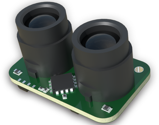
The applications for these advanced chips are vast and growing. In automotive, they are the enabling technology for solid-state LiDAR in advanced driver-assistance systems (ADAS) and autonomous vehicles. In consumer electronics, they enable facial recognition, gesture sensing, and augmented reality features in smartphones and tablets. Industrial robots use them for precise object detection, bin picking, and collision avoidance. In logistics, they power automated guided vehicles (AGVs) and volume measurement systems. The miniaturization and cost reduction driven by chip-level integration are unlocking new use cases in drones, smart home devices, and even healthcare monitoring equipment.
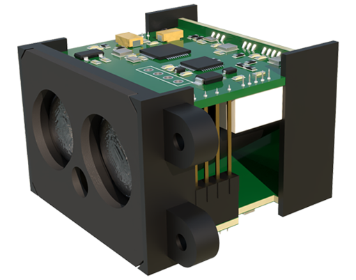
Looking ahead, the trajectory for laser ranging sensor chips points toward even higher levels of integration, lower power consumption, and enhanced functionality. We can expect the convergence of sensing and perception, where future chips will not only output distance point clouds but also perform initial on-chip processing for object classification and scene understanding. As semiconductor processes continue to shrink and novel materials like silicon photonics mature, the performance, affordability, and ubiquity of laser ranging will reach unprecedented levels, solidifying its role as a fundamental sensory modality for the intelligent machines of tomorrow.