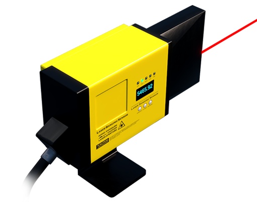
The production of laser gas sensors represents a sophisticated intersection of photonics, electronics, and precision engineering. These devices, crucial for industrial safety, environmental monitoring, and scientific research, rely on the principle of tunable diode laser absorption spectroscopy (TDLAS). The manufacturing journey begins long before assembly, rooted in meticulous design and material selection. Core components include a precisely tuned semiconductor laser diode, a photodetector, an optical path (often involving a gas cell or open path), and sophisticated signal processing electronics. The laser diode itself is engineered to emit light at a specific wavelength that corresponds to an absorption line of the target gas molecule, such as methane, carbon dioxide, or oxygen.
The fabrication process is typically segmented into several cleanroom-compatible stages. First, the laser diode chips are produced using epitaxial growth techniques like metalorganic chemical vapor deposition (MOCVD) on semiconductor wafers. This stage is critical for achieving the required wavelength stability and output power. Following dicing and testing, the diode is mounted onto a submount with precise thermal management, as even minor temperature fluctuations can shift the emission wavelength. Concurrently, the optical assembly is constructed. This involves aligning the laser, the sample gas cell (which may be a multi-pass cell to increase the absorption path length), and the photodetector with micron-level accuracy. Automated active alignment systems are often employed, where the optical power is monitored in real-time while components are adjusted to maximize coupling efficiency.
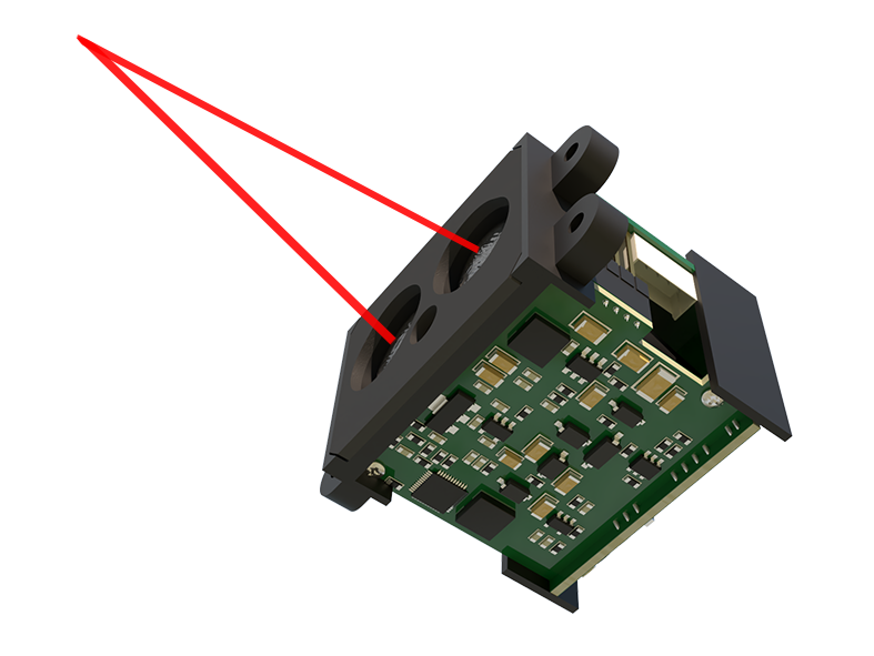
The electronic subsystem is equally vital. A driver circuit provides stable current and temperature control to the laser diode, often using a thermo-electric cooler (TEC) and a feedback loop. The signal from the photodetector, which carries the absorption information, is extremely weak. Therefore, a low-noise transimpedance amplifier (TIA) is designed and integrated to convert the photocurrent into a measurable voltage. Advanced digital signal processors (DSP) or microcontrollers then execute wavelength modulation spectroscopy (WMS) algorithms. In WMS, the laser's wavelength is rapidly modulated, allowing the system to detect the subtle absorption features against background noise, significantly enhancing sensitivity and selectivity.
Assembly and packaging present significant challenges, as the final product must be robust for field deployment. Hermetic sealing is often necessary to protect sensitive optics and electronics from humidity, dust, and corrosive atmospheres. The housing material is chosen for mechanical stability, thermal properties, and sometimes for its inertness to the target gas. Connectors for power, data, and possibly gas sampling are integrated with high reliability. Each sensor unit undergoes a rigorous calibration process using certified gas mixtures in controlled environmental chambers. This step establishes the sensor's response curve, ensuring accurate concentration readings across its specified range.

Quality control is embedded throughout the manufacturing pipeline. Incoming materials are inspected, in-process testing verifies sub-assembly performance, and final validation tests assess key parameters: detection limit, response time, cross-sensitivity to interfering gases, long-term stability (drift), and performance under varying temperature and pressure. Manufacturers adhere to international standards such as IEC 60079 for explosive atmospheres or performance standards specific to application areas like stack emissions monitoring.
The evolution of manufacturing trends is pushing the boundaries of laser gas sensor technology. The integration of photonic integrated circuits (PICs) aims to miniaturize the optical bench onto a single chip, promising smaller, more cost-effective, and more reliable sensors. Furthermore, the rise of the Industrial Internet of Things (IIoT) drives demand for sensors with integrated digital communication protocols (like IO-Link or WirelessHART) and self-diagnostic capabilities. Advanced manufacturing techniques, including automated optical inspection and machine learning for predictive quality analytics, are becoming standard to ensure consistency and yield in high-volume production. Ultimately, the goal of manufacturing is to deliver a sensor that provides unwavering accuracy and reliability, enabling safer workplaces, cleaner environments, and more efficient industrial processes.