Photoelectric proximity sensors are indispensable components in modern industrial automation, offering non-contact detection of objects based on light modulation. Understanding their schematic design is crucial for engineers to optimize performance in diverse applications, from packaging lines to robotic assembly. This article delves into the core principles and circuit configurations that define these sensors, providing a technical overview aligned with industry standards.
At the heart of a photoelectric proximity sensor lies three primary elements: an emitter (light source), a receiver (photodetector), and signal processing circuitry. The emitter typically employs a light-emitting diode (LED) that projects modulated infrared or visible light. Common modulation frequencies range from a few kHz to several hundred kHz, which helps mitigate interference from ambient light. The receiver, often a phototransistor or photodiode, detects the reflected or interrupted light beam. In a typical schematic, the emitter circuit includes a current-limiting resistor in series with the LED to prevent overdrive, while the receiver circuit incorporates amplification stages to process weak signals.
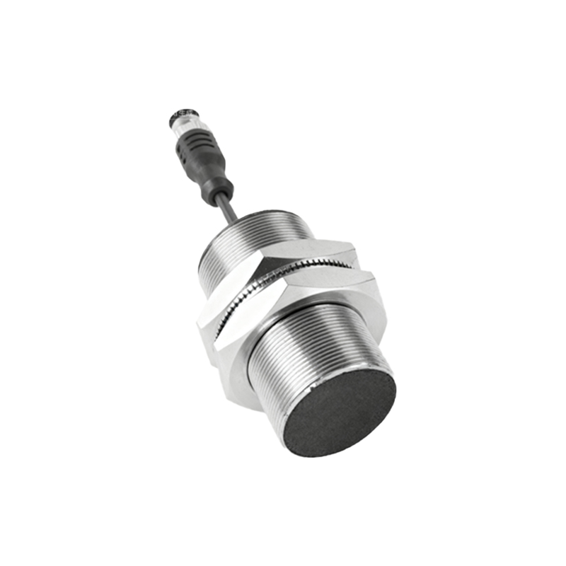
Schematics vary based on sensing modes. The through-beam (or opposed) mode uses separate emitter and receiver units facing each other; the schematic shows independent power supplies and output circuits for each unit. When an object interrupts the light path, the receiver’s output transitions, triggering a response. The retro-reflective mode integrates emitter and receiver in one housing, with a reflector bouncing light back. Its schematic includes components to filter out reflections from shiny objects, often using polarization filters. The diffuse (proximity) mode, where the sensor detects light reflected directly from the target, features the most complex circuitry. Here, schematics highlight sensitivity adjustments and background suppression techniques, such as triangulation-based circuits that ignore distant objects.
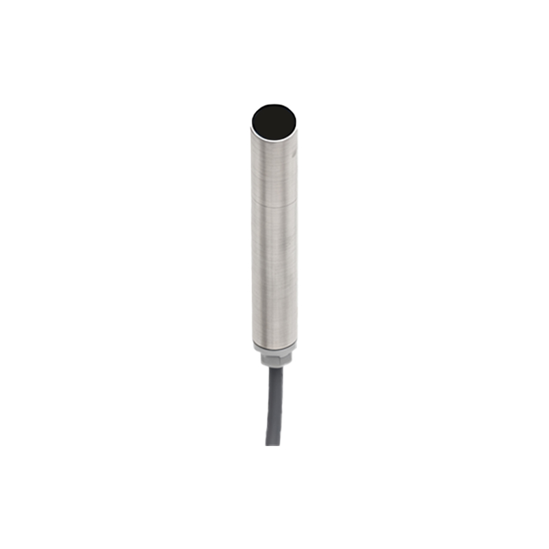
Key circuit blocks in a standard schematic include:
1. Oscillator and Driver: Generates pulsed light to reduce power consumption and enhance noise immunity.
2. Amplifier Stage: Boosts the receiver’s signal using operational amplifiers or transistor arrays.

3. Comparator: Compares the amplified signal to a threshold voltage, producing a clean digital output (e.g., NPN/PNP transistor outputs).
4. Output Interface: Provides switching capabilities (e.g., open-collector or relay outputs) to interface with PLCs or controllers.
5. Protection Circuits: Incorporate reverse polarity protection, surge suppression, and short-circuit safeguards.
Modern sensors integrate ICs like ASICs (Application-Specific Integrated Circuits) for compact designs. Schematics may show microcontrollers for programmability, enabling adjustments to sensing range or output delay. For instance, time-of-flight (ToF) sensors use precise timing circuits to measure distance by calculating light travel time.
When interpreting schematics, engineers must consider factors like supply voltage (typically 10-30 V DC), output current ratings, and response time. Environmental robustness is achieved through filtering components that handle dust or moisture interference. Maintenance tips include checking optical alignment in schematics to ensure emitter-receiver synchronization and verifying signal integrity with oscilloscopes.
In summary, photoelectric proximity sensor schematics reveal a blend of optical and electronic engineering. Mastery of these diagrams allows for effective troubleshooting, customization, and integration into automated systems, driving efficiency in industries like automotive, food processing, and logistics. As technology evolves, schematics continue to incorporate smart features, such as IO-Link communication modules, expanding their role in the Industrial Internet of Things (IIoT).