Laser cutting has emerged as a pivotal manufacturing process in the production of high-precision sensors, enabling the fabrication of intricate components with exceptional accuracy and minimal thermal distortion. This article delves into the core principles of laser cutting as applied to sensor manufacturing, exploring the physics, methodologies, and industry-specific considerations that electrical engineers must understand.
The fundamental principle of laser cutting involves focusing a high-energy laser beam onto a small spot on the workpiece material. For sensor components, common materials include various metals (stainless steel, aluminum alloys, copper), semiconductors (silicon), and specialized polymers. The intense energy density at the focal point rapidly heats the material, causing it to melt, vaporize, or be blown away by a high-pressure assist gas, thereby creating a precise kerf. The three primary mechanisms are vaporization cutting, melt and blow cutting, and thermal stress cracking, with the first two being most prevalent for sensor substrates and housings.
A critical component is the laser source itself. For sensor fabrication, fiber lasers and CO2 lasers are predominantly used. Fiber lasers, with wavelengths around 1.06 µm, are highly absorbed by metals and are excellent for cutting thin to medium-thickness metal sheets used in sensor diaphragms, strain gauges, and casings. They offer superior beam quality, leading to narrower kerfs and sharper edges, which is crucial for miniaturized sensor elements. CO2 lasers (wavelength ~10.6 µm) are often employed for cutting non-metallic materials and thicker metals, though their absorption by highly reflective metals like copper can be less efficient without specific surface treatments.
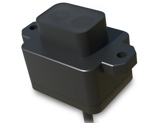
The cutting process is governed by several key parameters that engineers must optimize for sensor quality:
1. Laser Power: Determines the energy input. For delicate sensor parts, lower power with high pulse frequencies is often used for controlled ablation.
2. Cutting Speed: Affects the heat input per unit length. Too slow can cause excessive heat-affected zones (HAZ), potentially altering the material's mechanical or electrical properties—a critical concern for sensing elements.
3. Assist Gas: Type and pressure are vital. Oxygen is used for exothermic reactions to cut mild steel, but for sensor metals where oxidation must be avoided (e.g., to prevent signal drift or corrosion), inert gases like nitrogen or argon are standard. The gas also ejects molten material, preventing dross on the cut edge.
4. Focal Point Position: Precisely controlling the beam's focal point relative to the material surface is essential for achieving the desired kerf width and edge quality. A negative defocus (focus below the surface) is often used for thicker materials.
In sensor manufacturing, edge quality is paramount. A smooth, perpendicular cut edge with minimal HAZ ensures structural integrity and reliable performance. Burr formation must be eliminated, as micro-burrs can interfere with assembly, cause stress concentrations, or even affect electrical contacts in sensing circuits. Advanced techniques like pulsed-wave cutting and adaptive optics are employed to achieve such high-quality edges, especially for fragile materials like piezoelectric ceramics or silicon wafers used in MEMS sensors.
Furthermore, the integration of Computer Numerical Control (CNC) and CAD/CAM software allows for the cutting of complex 2D and 3D geometries from sensor design files with micron-level precision. This is indispensable for producing components like comb drives for capacitive sensors, micro-machined diaphragms for pressure sensors, or intricate patterns for optical sensors. The non-contact nature of laser cutting eliminates tool wear and mechanical stress, preserving the delicate features of these microstructures.
A significant advantage for electrical engineers designing sensors is the process's compatibility with automation. Laser cutting systems can be seamlessly integrated into production lines, enabling high-volume manufacturing of consistent sensor parts. This repeatability is critical for maintaining calibration and sensitivity across sensor batches.
However, challenges persist. Reflective materials like copper or gold (used in conductive traces) can reflect laser energy, reducing efficiency and potentially damaging the optics. Anti-reflection coatings or using lasers with specific wavelengths (e.g., green lasers for copper) are common solutions. Thermal management is also crucial; excessive heat can induce micro-cracks or alter the temper of metals, affecting long-term sensor stability.
In conclusion, laser cutting is a sophisticated, versatile, and essential technology in modern sensor fabrication. Its ability to produce clean, precise, and complex geometries in a wide range of materials makes it the process of choice for developing the next generation of high-performance, miniaturized sensors. For electrical engineers, a deep understanding of its principles—from beam-material interaction to parameter optimization—is key to designing sensor components that are not only functional but also manufacturable with the high fidelity required for reliable operation in demanding applications.