In the rapidly evolving landscape of sensor manufacturing, laser cutting has emerged as a cornerstone technology, enabling unprecedented levels of precision, efficiency, and design flexibility. This advanced fabrication process utilizes a focused, high-energy laser beam to cut, engrave, or shape various materials essential for sensor components, such as metals, ceramics, polymers, and composites. The non-contact nature of laser cutting eliminates mechanical stress and tool wear, which is critical for producing the delicate and intricate features required in modern sensors, including micro-electromechanical systems (MEMS), pressure diaphragms, and optical sensor grids.
The core principle involves directing a concentrated beam of light, typically from CO2, fiber, or ultrafast lasers, onto the workpiece. The material at the point of interaction absorbs the laser energy, leading to rapid heating, melting, and vaporization. Computer Numerical Control (CNC) systems guide this process with micron-level accuracy, translating digital designs into physical parts with exceptional repeatability. For sensor applications, this translates to clean, burr-free edges, minimal heat-affected zones (HAZ), and the ability to achieve complex geometries that are impossible with conventional mechanical cutting.
Key advantages of laser cutting in sensor production are manifold. Firstly, it offers superior precision, with cutting widths often below 20 micrometers, allowing for the miniaturization of sensor elements. This is vital for applications in medical devices, aerospace, and consumer electronics where space is at a premium. Secondly, the process is highly versatile and agile. Switching between different cutting patterns or materials requires only a change in the digital program, drastically reducing setup times and enabling cost-effective low-volume or prototype production runs. Thirdly, laser systems can process a wide range of material thicknesses, from thin foils to several millimeters, making them suitable for diverse sensor housings and internal structures.
Recent innovations are pushing the boundaries further. Ultrafast picosecond and femtosecond lasers are gaining traction for processing sensitive materials. Their extremely short pulse durations deliver energy before significant heat conduction occurs, virtually eliminating the HAZ and thermal distortion. This "cold ablation" process is ideal for cutting brittle materials like silicon or glass used in optical and environmental sensors, preserving their intrinsic material properties. Additionally, the integration of in-process monitoring systems, such as vision inspection and real-time beam diagnostics, ensures consistent quality and immediate detection of defects, enhancing overall yield and reliability.

Despite its benefits, implementing laser cutting requires careful consideration. Material selection is paramount, as different substrates interact uniquely with laser wavelengths. Engineers must optimize parameters like power, pulse frequency, cutting speed, and assist gas (e.g., nitrogen, oxygen) to achieve the desired edge quality and throughput. Furthermore, initial capital investment for high-end laser systems can be significant, though the long-term gains in precision, speed, and reduced waste often justify the cost for high-value sensor manufacturing.
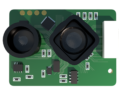
Looking ahead, the convergence of laser cutting with Industry 4.0 and smart manufacturing trends is set to deepen. Automated laser cells, integrated with robotics and IoT connectivity, will enable lights-out production with real-time data analytics for predictive maintenance and process optimization. As sensor technologies advance towards greater integration and functionality, laser cutting will remain an indispensable tool, driving innovation by allowing engineers to materialize increasingly sophisticated and reliable sensor designs that power the intelligent systems of tomorrow.