In the rapidly advancing fields of industrial automation, scientific research, and defense technology, the interaction between high-power laser systems and sensitive photodetectors or imaging sensors is increasingly common. A critical challenge that arises in these environments is the potential for laser-induced sensor damage. This phenomenon is not merely an operational nuisance but a significant reliability and safety concern that can lead to costly equipment failure, data corruption, and system downtime. This article delves into the fundamental mechanisms behind laser damage, explores the types of sensors most at risk, and outlines practical prevention strategies and industry-standard solutions.
The core mechanism of laser damage to sensors is the deposition of excessive optical energy onto the detector's active area, exceeding its material and design limits. This energy transfer can occur through several distinct physical processes, often in combination. The most common is thermal damage. When a laser beam, even a low-power continuous-wave (CW) laser if focused tightly, irradiates a pixel or the sensor surface, the absorbed energy converts to heat. If the heat cannot dissipate quickly enough through the sensor's substrate and packaging, localized temperatures can soar. This can melt metallic interconnects, cause delamination of micro-lens arrays, create thermal stress cracks in silicon, or permanently alter the semiconductor's doping properties, leading to "hot pixels" or complete pixel death.
A second, more instantaneous mechanism is dielectric breakdown, often associated with high-peak-power pulsed lasers, such as Q-switched or mode-locked systems. The intense electric field of an ultrashort pulse can directly ionize the semiconductor material, creating a plasma and causing catastrophic structural failure at the atomic level. This type of damage is often characterized by microscopic pits or cratering on the sensor surface. Furthermore, photochemical effects, though less common with silicon-based sensors, can degrade certain coatings or organic materials used in specialized detectors over prolonged exposure to specific wavelengths, even at lower power levels.
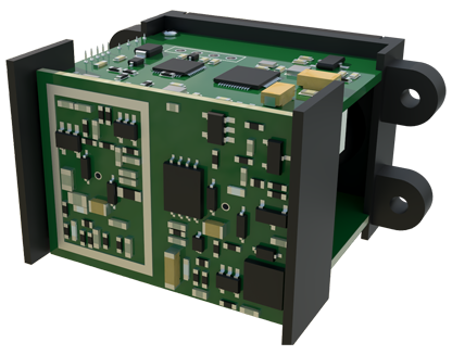
Not all sensors are equally vulnerable. The risk profile depends heavily on the sensor technology. Charge-Coupled Device (CCD) and Complementary Metal-Oxide-Semiconductor (CMOS) image sensors, the workhorses of digital imaging, are highly susceptible due to their dense, light-sensitive pixel arrays. Photodiodes, including avalanche photodiodes (APDs) and PIN diodes, have defined damage thresholds but can be easily overloaded. Even non-optical sensors, like position-sensitive detectors (PSDs) or certain MEMS devices, can be impaired if their functional elements are exposed to stray laser light. Key factors influencing the damage threshold include laser wavelength (relative to the sensor's spectral response), pulse duration (CW vs. nanosecond vs. femtosecond), beam diameter and profile, and the sensor's inherent optical coating and passivation layers.
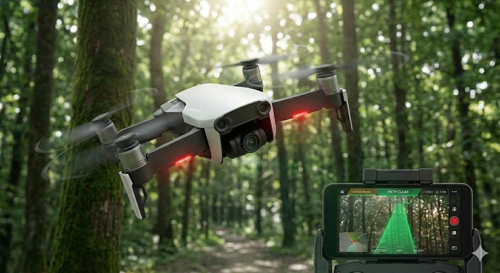
Preventing laser damage is a multi-layered engineering discipline, starting at the system design phase. The primary and most effective defense is optical isolation and attenuation. This involves the strategic use of bandpass or notch filters that block the specific laser wavelength while transmitting the desired signal light. Neutral density (ND) filters can be employed to attenuate beam intensity to a safe operational level. For environments with unpredictable or reflected beams, physical beam dumps, shrouds, and apertures are essential to contain stray light.
Electronic safeguards form the second line of defense. Many modern sensor modules and cameras incorporate automatic exposure control (AEC) and optical power monitoring circuits that can react within microseconds to shut a protective shutter or trigger an alarm when an unsafe light level is detected. For pulsed laser environments, synchronizing the sensor's readout or gating its active period to the laser-off phase is a sophisticated but highly effective technique.
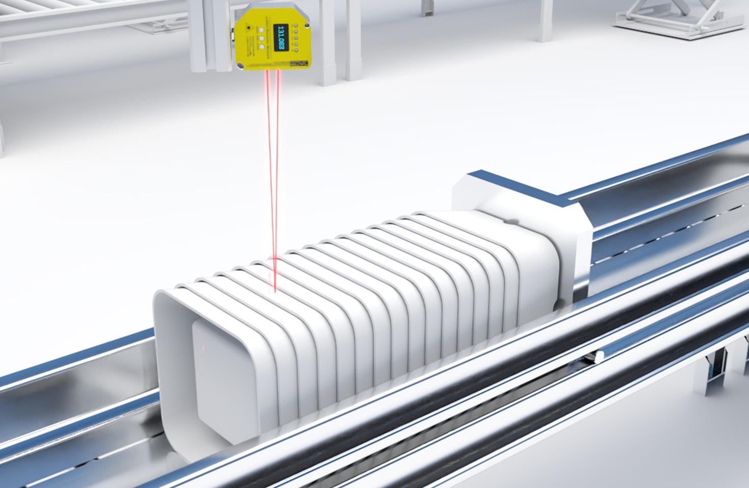
From an operational and maintenance standpoint, rigorous procedural controls are indispensable. This includes comprehensive operator training on laser safety (aligned with standards like ANSI Z136.1), clear labeling of laser zones and sensor apertures, and regular inspection of optical components for degradation or contamination that might increase absorption and susceptibility to damage. Implementing interlocks that disable high-power laser emission when a sensor access panel is open is a standard safety practice.
The industry continues to innovate in material science and sensor design to push damage thresholds higher. Research into wide-bandgap semiconductors like gallium nitride (GaN) or silicon carbide (SiC) for UV and high-power applications shows promise. Advanced anti-reflective (AR) coatings with higher laser-induced damage thresholds (LIDT) are being developed. Furthermore, system-level solutions, such as using sacrificial, replaceable sensor heads in extreme environments or implementing redundant sensor arrays with voting logic, are employed in critical applications.
In conclusion, laser damage to sensors is a well-understood but ever-present risk in high-tech industries. Mitigation requires a holistic approach combining an understanding of the failure physics, careful component selection with certified LIDT data, intelligent system design with multiple protective layers, and strict adherence to safety protocols. By integrating these principles, engineers can ensure sensor longevity, data integrity, and the safe, reliable operation of systems where powerful lasers and sensitive detectors must coexist.