In the realm of industrial automation and precision measurement, CMOS laser sensors represent a critical fusion of optical engineering and semiconductor technology. This teardown analysis provides an in-depth examination of a typical industrial-grade CMOS laser sensor, revealing the design principles, component selection, and integration techniques that enable high-performance operation in demanding environments.
The external housing, constructed from anodized aluminum alloy, provides both electromagnetic shielding and thermal dissipation. Upon removal, the internal architecture is organized into three primary modules: the laser emission unit, the optical reception path, and the signal processing board. The laser diode, typically a Class 2 visible red or infrared type, is mounted on a thermally stabilized submount. It is driven by a constant-current circuit with active temperature compensation, ensuring wavelength stability crucial for measurement accuracy. Adjacent to the diode, a collimating lens assembly, often an aspheric element, shapes the divergent beam into a precise, low-divergence output.
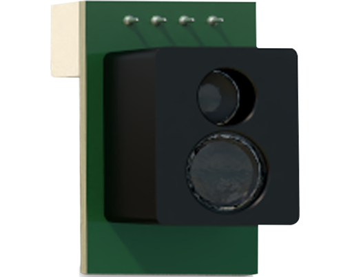
The core of the reception system is the CMOS linear image sensor. This is not a standard consumer camera sensor but a specialized chip with a high dynamic range and on-chip timing generation. It is positioned behind a receiving lens that focuses the reflected laser spot onto its pixel array. The sensor's pixel pitch and total pixel count directly determine the sensor's theoretical resolution and measurement range. Notably, the optical path includes a narrow-bandpass interference filter placed directly in front of the sensor. This filter is meticulously tuned to the laser's emission wavelength, dramatically attenuating ambient light interference—a key feature for reliable operation under variable factory lighting conditions.
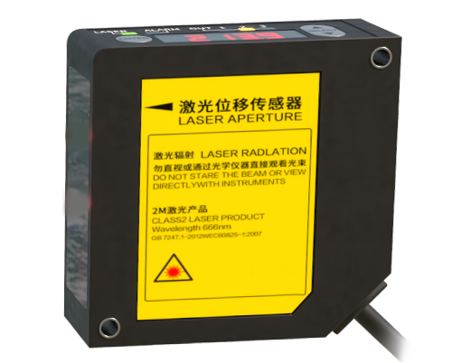
The signal processing printed circuit board (PCB) is a multilayer design with separate ground planes for analog and digital sections to minimize noise. Central to this board is a dedicated microcontroller or DSP (Digital Signal Processor). This processor executes proprietary algorithms for sub-pixel interpolation, calculating the centroid position of the laser spot on the CMOS array with resolution finer than a single pixel. Supporting circuitry includes a high-precision analog-to-digital converter (ADC) for digitizing the sensor's analog output, voltage regulators with low noise characteristics, and robust digital communication interfaces (e.g., RS-485, Ethernet/IP, or IO-Link). The power supply section often incorporates reverse-polarity and overvoltage protection.
Key observations from component-level analysis highlight the engineering trade-offs. The choice of CMOS technology over CCD (Charge-Coupled Device) is deliberate, offering advantages in lower power consumption, faster readout speeds, and easier system integration. However, managing the inherent higher noise floor of CMOS sensors is addressed through correlated double sampling circuitry on the chip and sophisticated digital filtering in the firmware. The mechanical design shows precise alignment features, with set screws and epoxy locking for the optical elements to maintain calibration against vibration and thermal cycling.
Performance validation in a controlled setting involves checking parameters like repeatability, linearity error, and response time. The sensor's output is typically a digital value representing distance or presence, calibrated against traceable standards. Understanding this internal architecture is vital for engineers specifying, integrating, and maintaining these systems. It explains the sensor's limitations (e.g., minimum sensing distance, effects of target surface color and texture) and informs best practices for installation, such as avoiding optical contamination and ensuring stable electrical grounding.
Future trends observable in newer designs include the integration of more advanced processors enabling multi-point measurement and profile analysis, the adoption of VCSEL (Vertical-Cavity Surface-Emitting Laser) light sources for enhanced reliability, and the implementation of functional safety features directly within the sensor module. This teardown underscores that the reliability of a CMOS laser sensor is not defined by a single component but by the synergistic integration of precision optics, robust electronics, and intelligent software.